Electroluminescent display

a technology of el display and el-type, which is applied in the direction of discharge tube/lamp details, discharge tube luminescnet screens, organic semiconductor devices, etc., can solve the problem of constructive interference in and achieve the enhancement of light emission characteristics such as luminance, light efficiency, and chromaticity.

Active Publication Date: 2005-01-20
SAMSUNG DISPLAY CO LTD
View PDF4 Cites 43 Cited by
  • Summary
  • Abstract
  • Description
  • Claims
  • Application Information

AI Technical Summary

Benefits of technology

[0007] The present invention provides an EL display in which light emitted from a light-emitting layer undergoes constructive interference due to a resonance effect. As a result, the EL display enhances light emission characteristics such as luminance, light efficiency, and chromaticity. The present invention also provides an EL display that can adjust the amount of light emitted from an anode and a cathode.

Problems solved by technology

However, since light emitted from the light-emitting layer 33 is not reflected by the anode 20 or the cathode 40, it is impossible to accomplish the enhancement of light emission characteristics by constructive interference due to a resonance effect of light emitted from the light-emitting layer 33.

Method used


Image

  • Electroluminescent display
  • Electroluminescent display
  • Electroluminescent display

Examples


example 1

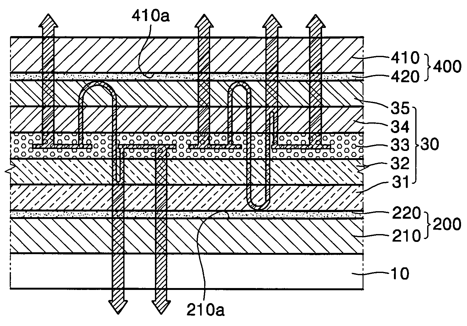
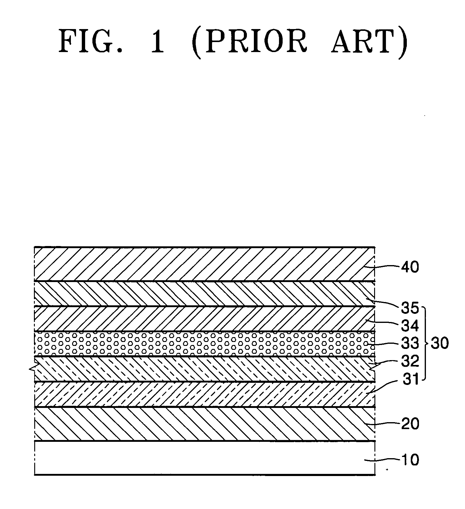
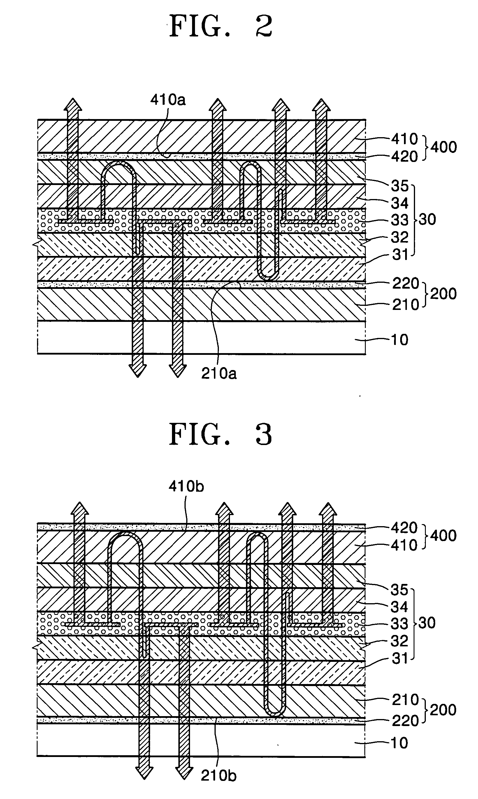
[0037] An EL display was prepared including the transparent substrate 10, the first transparent conductive layer 210 made of ITO on the transparent substrate 10, the first partially reflective layer 220 (20 nm thickness) made of Ag on the first transparent conductive layer 210, the hole injection layer 31 (10 nm thickness) made of CuPc on the first partially reflective layer 220, the hole transport layer 32 (50 nm thickness) made of N,N′-di(1-naphtyl)-N,N′-diphenylbenzidine (NPD) on the hole injection layer 31, the light-emitting layer 33 (30 nm thickness) made of carbazole biphenyl (CBP) doped with 5% tris (fac-phenylpyridien) iridium on the hole transport layer 32, a hole blocking layer (5 nm thickness) made of biphenoxy-bi(8-quinolinolato)aluminum (BAlq) on the light-emitting layer 33, the electron transport layer 34 (20 nm thickness) made of tris(8-quinolinolato)aluminum (Alq) on the hole blocking layer, the electron injection layer 35 (0.5 nm thickness) made of LiF on the elect...


PUM


Abstract

An EL display is provided with enhanced light emission characteristics wherein light emitted from a light-emitting layer undergoes constructive interference due to a resonance effect. The EL display includes a transparent substrate, an anode and a cathode formed on the same side of the transparent substrate, and an intermediate layer interposed between the anode and the cathode, and said intermediate layer including a light-emitting layer that emits light when the anode and the cathode are electrically driven by a voltage, and wherein the anode and the cathode are formed as a translucent conductive layer that partially reflects the light emitted from the light-emitting layer.

Description

CROSS-REFERENCE TO RELATED APPLICATIONS [0001] This application claims priority of Korean Patent Application No. 2003-49543, filed on Jul. 19, 2003, and No. 2003-54794, filed on Aug. 7, 2003, in the Korean Intellectual Property Office, both of which hereby are incorporated by reference. BACKGROUND OF THE INVENTION [0002] 1. Field of the Invention [0003] The present invention relates to an electroluminescent display (EL), and more particularly, to a bi-directional emission-type EL display. [0004] 2. Description of the Related Art [0005] EL displays are active light-emitting display devices that have numerous advantages over cathode ray tubes (CRTs) or liquid crystal displays (LCDs). EL displays can provide a wider viewing angle, higher contrast, faster response speed, lighter weight, smaller size, thinner thickness, and lower power consumption. There is an increasing interest on developing EL displays as next generation displays. EL displays are classified into inorganic and organic ...

Claims


Application Information

Patent Timeline
Patent Type & Authority Applications(United States)
IPC IPC(8): H01J1/62H05B33/24H01L51/00H01L51/50H01L51/52H05B33/12H05B33/14H05B33/28
CPCH01L51/0059H01L51/0062H01L51/0081H01L2251/5323H01L51/5206H01L51/5221H01L51/5265H01L51/0085H10K59/17H10K85/631H10K85/649H10K85/324H10K85/342H10K50/816H10K50/828H10K50/852H10K2102/3031
Inventor LEE, JUN-YEOBLEE, HAN-JUOH, JUN-SIK
Owner SAMSUNG DISPLAY CO LTD
Why Eureka
Try Eureka