Active matrix organic electroluminescent display device and method of fabricating the same

Active Publication Date: 2005-01-20
LG DISPLAY CO LTD
View PDF13 Cites 30 Cited by
  • Summary
  • Abstract
  • Description
  • Claims
  • Application Information

AI Technical Summary

Benefits of technology

[0025] An object of the present invention is to provide an active matrix OELD device having a driving thin film transistor arrangement in a pixel with decreas

Problems solved by technology

The passive matrix type has a simple structure and fabrication process, but has a high power consumption as compared to the active matrix type.
Further, because the display size of passive matrix organic electroluminescent display devices is limited by its structure, the passive matrix type can not easily be adapted to a large sized device.
Further, since a large amount of current flows through the driving thin film transistor TD, current stress may be caused in the driving thin film transistor TD, thereby damaging the driving thin film transistor

Method used


Image

  • Active matrix organic electroluminescent display device and method of fabricating the same
  • Active matrix organic electroluminescent display device and method of fabricating the same
  • Active matrix organic electroluminescent display device and method of fabricating the same

Examples


Embodiment Construction

[0041] Reference will now be made in detail to the preferred embodiments of the present invention, examples of which are illustrated in the accompanying drawings. Wherever possible, similar reference numbers will be used throughout the drawings to refer to the same or like parts.

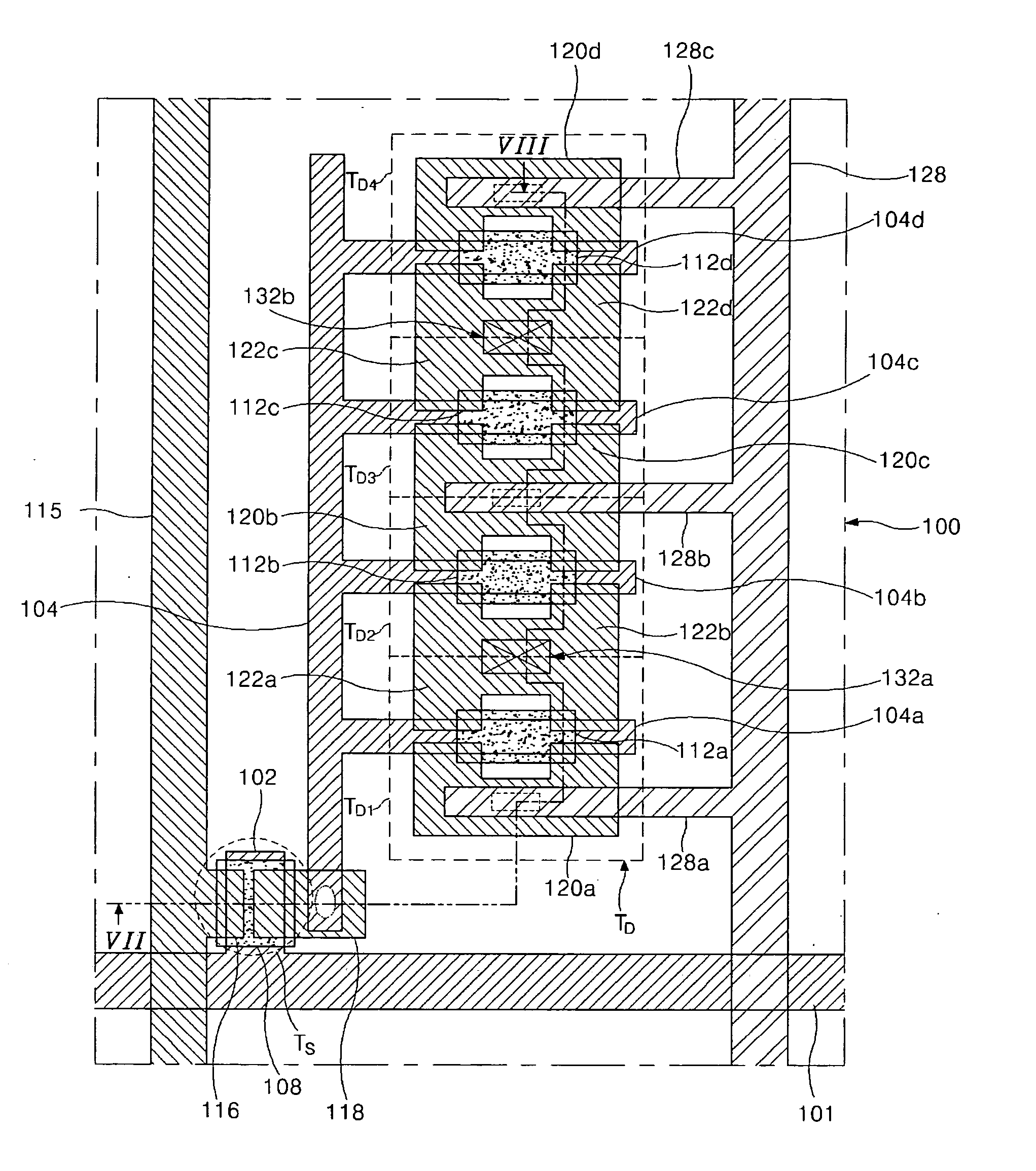
[0042]FIG. 6 is a schematic plan view of a pixel of an exemplary active matrix organic electroluminescent display device according to the present invention. The active matrix organic electroluminescent display device of FIG. 6 is a top emission type unlike the related art of FIG. 3. A gate line 101 crosses a data line 115 and a power line 128, which are spaced apart from each other. A pixel region is defined between the gate line 101 and the spaced apart data and power supply lines 115 and 128. A switching thin film transistor (TFT) TS is disposed adjacent to where the gate line 101 and the data line 115 cross each other. A driving thin film transistor (TFT) TD is disposed in the pixel region between the da...


PUM


Abstract

An organic electroluminescent display device includes a substrate, a gate line on the substrate, a data line crossing the gate line over the substrate, a switching thin film transistor near the crossing of the gate line and data line, a driving thin film transistor system including a plurality of sub-TFTs connected in parallel to the switching thin film transistor via a gate base, a power line crossing the gate line over the substrate and electrically connected with the plurality of sub-TFTs, a first electrode over the driving thin film transistor system in contact with the plurality of sub-TFTs, an organic electroluminescent layer on the first electrode, and a second electrode of transparent material on the organic electroluminescent layer.

Description

[0001] The present invention claims the benefit of Korean Patent Application No. 2002-0088417 filed in Korea on Dec. 31, 2002, which is hereby incorporated by reference. BACKGROUND OF THE INVENTION [0002] 1. Field of the Invention [0003] The present invention relates to a display device and a method of fabricating a display device, and more particularly, to an active matrix organic electroluminescent display device and method of fabricating an active matrix organic electroluminescent display device. [0004] 2. Discussion of the Related Art [0005] An organic electroluminescent display device includes a cathode electrode to inject electrons, an anode electrode inject to holes, and an organic electroluminescent layer between the two electrodes. An organic electroluminescent diode has a multi-layer structure of organic thin films provided between the anode electrode and the cathode electrode. When a forward current is applied to the organic electroluminescent diode, electron-hole pairs (...

Claims


Application Information

Patent Timeline
IPC IPC(8): G09F9/30H04M3/22G09G3/32H01L21/77H01L21/84H01L27/12H01L27/32H01L51/50H01L51/56H05B33/00
CPCG09G3/3233G09G2300/0443G09G2300/0842H01L27/12H01L27/3244H01L27/3251H01L27/1248H01L27/3276H01L2251/5315H01L51/5212H01L51/5246H01L27/3253H01L27/3262H10K59/127H10K59/1275H10K59/12H10K59/1213H10K59/131H10K50/814H10K50/8426H10K2102/3026H05B33/00
Inventor PARK, JAE-YONGCHO, SO-HAENG
Owner LG DISPLAY CO LTD
Why Eureka
Try Eureka