

Method for fabricating copper interconnects
a technology of copper interconnects and manufacturing methods, applied in semiconductor/solid-state device manufacturing, basic electric elements, electric apparatus, etc., can solve the problems of poor adhesion of copper, short circuit, silicon nitride,
- Summary
- Abstract
- Description
- Claims
- Application Information
AI Technical Summary
Benefits of technology
Problems solved by technology
Method used
Image

Examples
Embodiment Construction
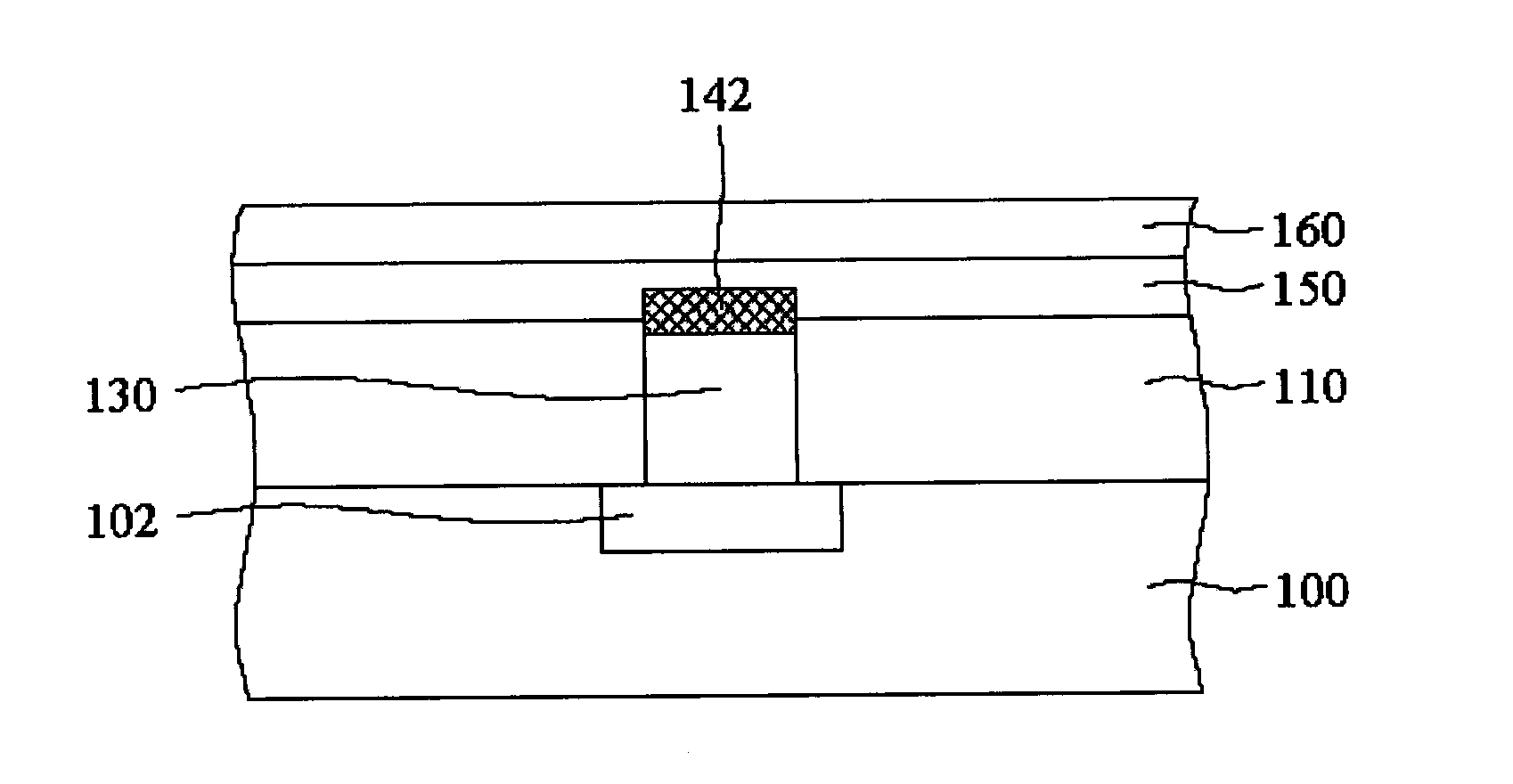
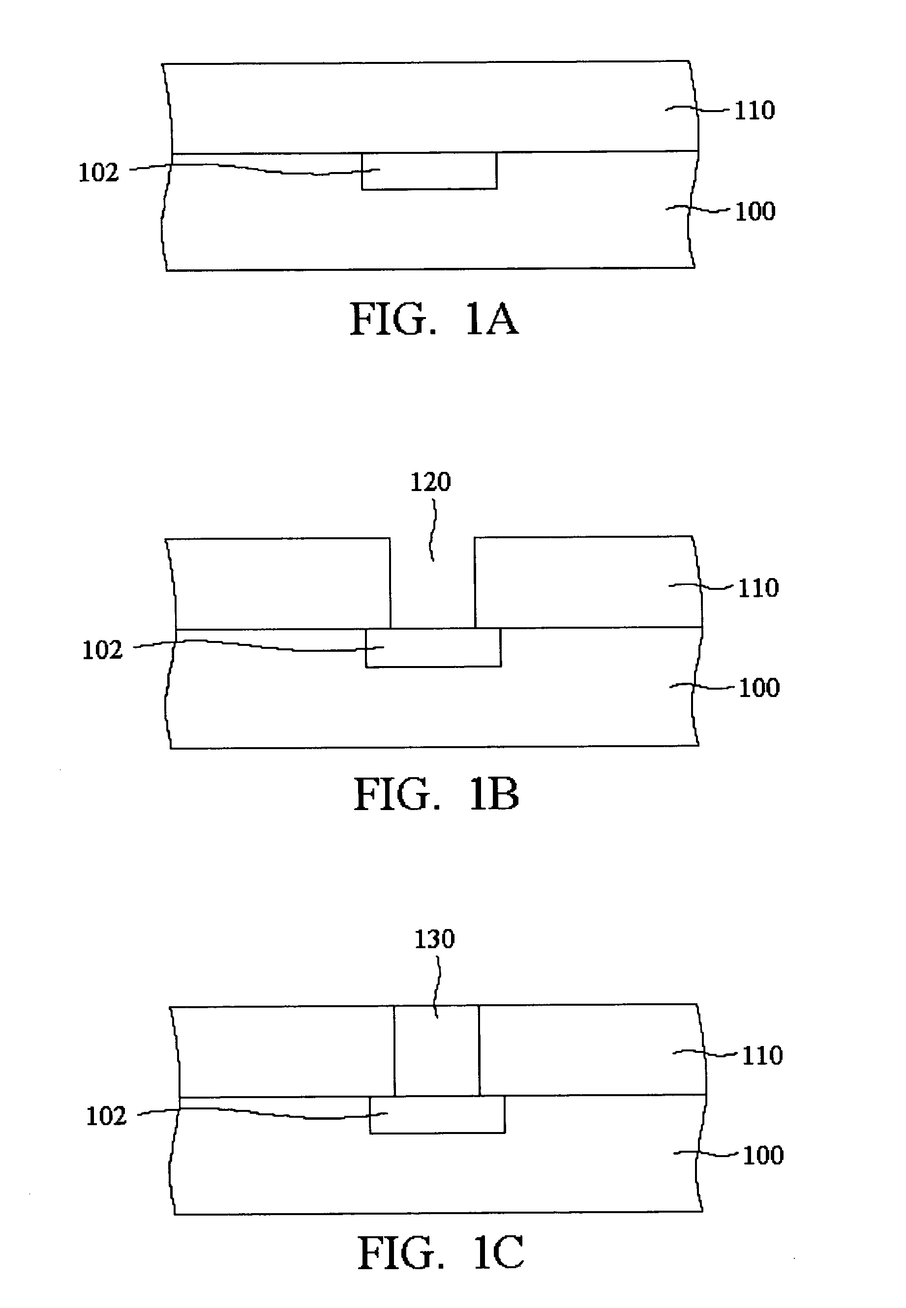
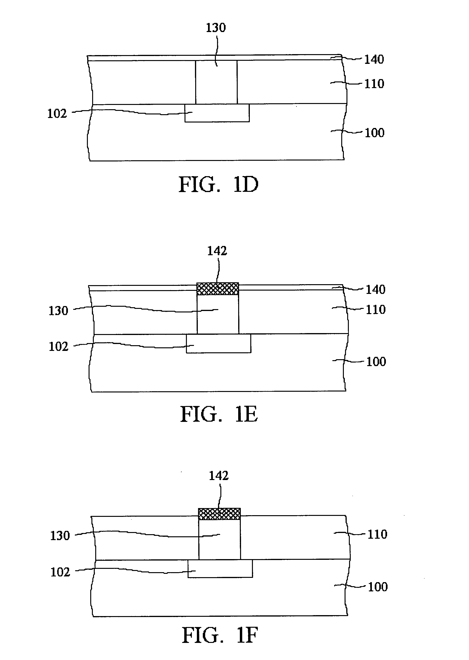
[0018] In FIG. 1A, a semiconductor substrate 100 is provided with a conductive structure 102 thereon, such as a gate electrode or a metal line. A dielectric layer 110 is deposited overlying the semiconductor substrate 100. The preferred dielectric layer 110 is low-k material (k≦3.2), such as organic low-k material, CVD low-k material, or a combination thereof The dielectric layer can also be fluorinated silica glass (FSG), SiC, SiOC, SiOCN, carbon-containing silicon oxide or nitrogen-containing silicon oxide.
[0019] A damascene opening 120 is subsequently formed within the dielectric layer 110 to expose the underlying conductive structure 102 as shown in FIG. 1B. The preferred width of the opening 120 is less than 900 Å. Preferably, the opening 120 is defined by a conventional dual damascene process to form a trench and a via opening.
[0020] The opening 120 is filled with copper or copper alloy to form a copper plug 130, as FIG. 1C shows. In one embodiment, a diffusion barrier layer...
PUM
 Abstract
Description
Claims
Application Information