Semiconductor memory device capable of reducing power consumption during reading and standby
a memory device and memory technology, applied in the direction of information storage, static storage, digital storage, etc., can solve the problems of power consumption of bit line charging/discharging operation, increased delay time, circuit complexity, etc., and achieve the effect of reducing power consumption
- Summary
- Abstract
- Description
- Claims
- Application Information
AI Technical Summary
Benefits of technology
Problems solved by technology
Method used
Image
Examples
first embodiment
[0034] First Embodiment
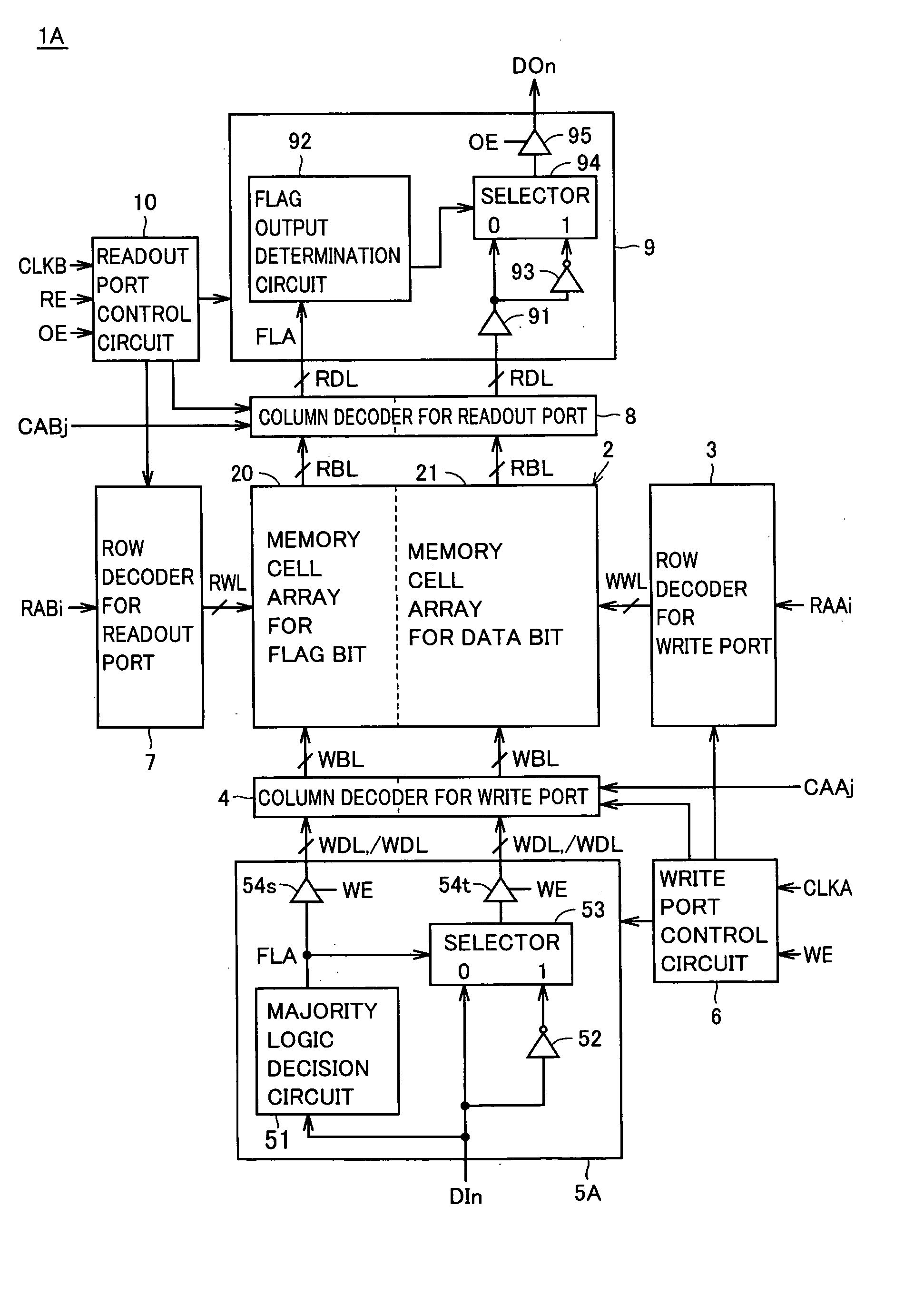
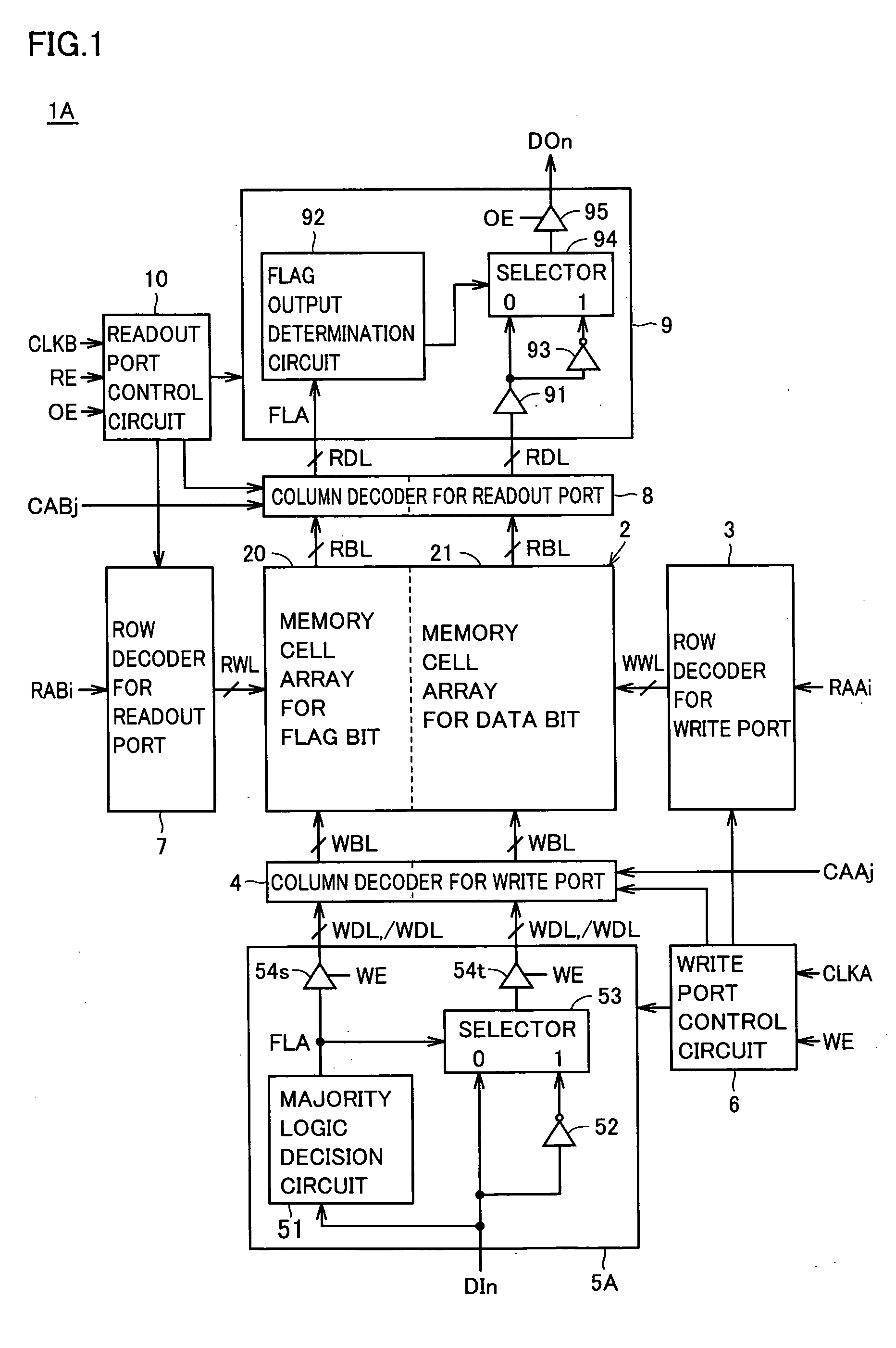
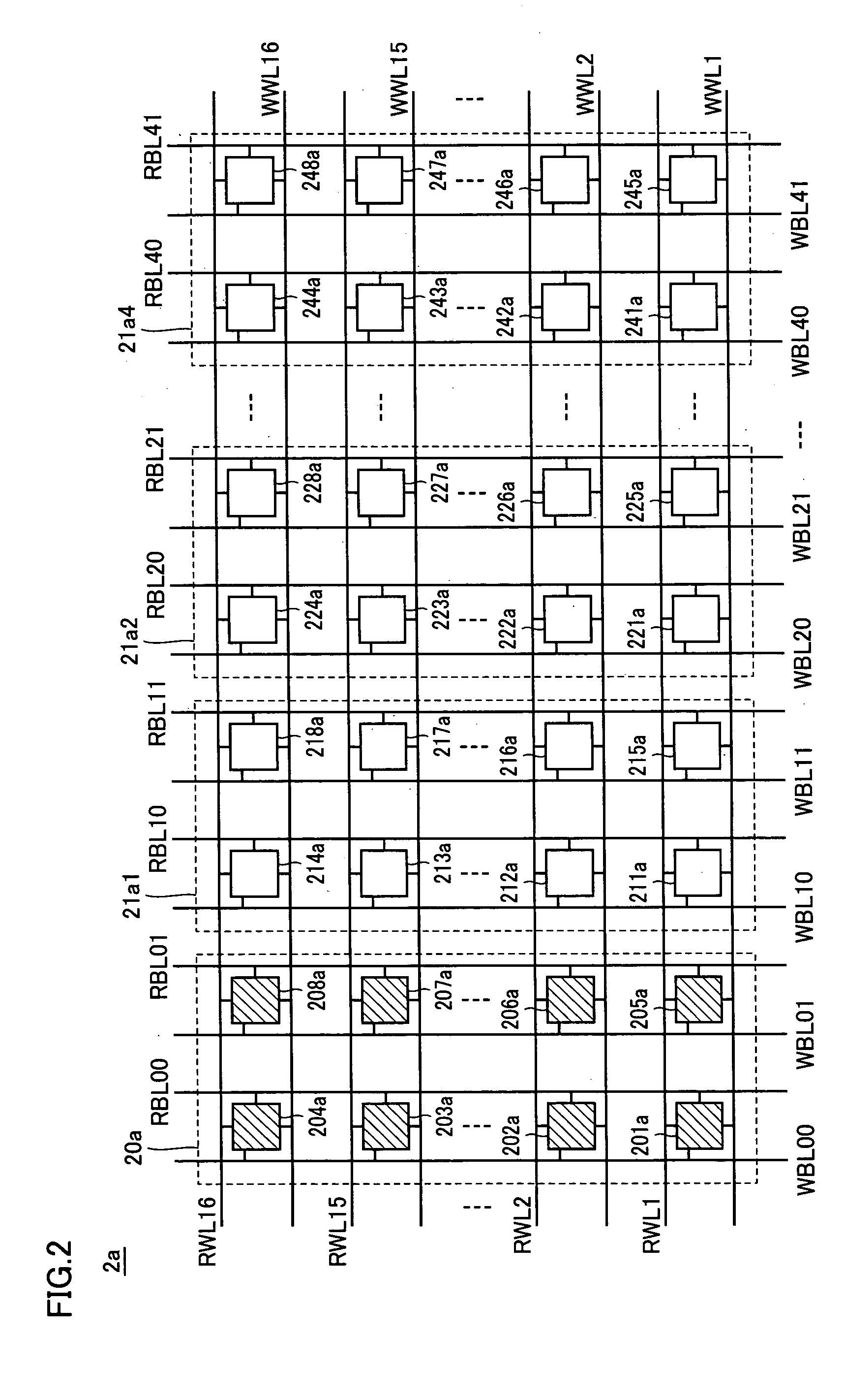
[0035] Referring to FIG. 1, a semiconductor memory device 1A according to a first embodiment of the present invention includes a memory cell array 2, a row decoder 3 for a write port, a column decoder 4 for a write port, a data input circuit 5A, a write port control circuit 6, a row decoder 7 for a readout port, a column decoder 8 for a readout port, a data output circuit 9, and a readout port control circuit 10. Memory cell array 2 is a 2-port memory cell array, including a flag bit memory cell array 20, and a data bit memory cell array 21. A specific configuration of memory cell array 2 will be described afterwards.
[0036] Write port row decoder 3 renders a corresponding write word line WWLi active in accordance with a row address signal RAAi (i=1−m:m is an integer of at least 0) for a write port. The subscript i may be omitted when the designation is provided generically.
[0037] Data input circuit 5A includes a majority logic decision circuit 51, an inverte...
second embodiment
[0135] Second Embodiment
[0136] Referring to FIG. 13, a semiconductor memory device 1B according to a second embodiment of the present invention differs from semiconductor memory device 1A of the first embodiment only in that data input circuit 5A is replaced with a data input circuit 5B. A detailed configuration of data input circuit 5B will be described hereinafter, and elements common to those of semiconductor memory device 1A will not be repeated.
[0137] Referring to FIG. 14, data input circuit 5B of the second embodiment includes write driver circuits 54a and 54bk (k=1−n), a selector 53_k, a flip-flop circuit 500_k, a sense amplifier 510 for majority logic decision, and a precharge circuit 550.
[0138] Precharge circuit 550 includes P channel MOS transistors 551 and 552 to precharge a pair of majority decision lines JL and / JL to an H level in synchronization with write port clock signal CLKA. Flip-flop circuit 500_k latches data input signal DIk (k=1−n) in synchronization with w...
PUM
 Abstract
Description
Claims
Application Information


