Semiconductor device fabrication method

a technology of semiconductor devices and fabrication methods, applied in the direction of manufacturing tools, grinding machine components, lapping machines, etc., can solve the problems of insufficient device isolation function, bird's beaks reducing device regions, and low polishing pressure, etc., to achieve accurate detection, low polishing pressure, and high polishing pressure

Inactive Publication Date: 2005-02-03
FUJITSU SEMICON LTD
View PDF13 Cites 10 Cited by
  • Summary
  • Abstract
  • Description
  • Claims
  • Application Information

AI Technical Summary

Benefits of technology

[0054] As described above, according to the present invention, in the finishing polish, not only deionized water but also the polishing slurry are supplied on to the polishing pad, a position for the polishing slurry to be supplied to and a position for the deionized water to be supplied to are suitably set, and a ratio of a supply amount of the polishing slurry and a supply amount of the deionized water is suitably set, whereby the intra-plane film thickness of the film-to-be-polished after finish-polished can be uniform.
[0055] According to the present invention, the finish of the finishing polish is detected based on a drive current or others of the polishing table or others, whereby the finish of the finishing polish can be accurately detected. Thus, according to the present invention, the residue of the film-to-be-polished on the device region and the occurrence of deep dishing in the surface of the buried insulation film of the film-to-be-polished can be prevented.
[0056] According to the present invention, in the first stage of the main polish, the film-to-be-polished is polished under a relatively high polishing pressure, and in the second stage of the main polish, the film-to-be-polished is polished under a relatively low polishing pressure. The film-to-be-polished is polished under a relatively high polishing pressure in the first stage polish, and the film-to-be-polished can be polished at a relatively high polishing rate. On the other hand, in the second stage polish, the film-to-be-polished is polished under a relatively low polishing pressure, whereby the surface of the film-to-be-polished can be sufficiently planarized. Thus. according to the present invention, the main polish period of time can be shortened without impairing the planarity of the film-to-be-polished.
[0057] According to the present invention, a plurality of inspection patterns of different areas are formed in advance, and based on a difference of film thicknesses of the buried insulation film forming these inspection patterns, whether or not the polish of the film-to-be-polished is normal is inspected, whereby even when the finishing polish is performed with the polishing slurry containing abrasive grains, and an additive of a surfactant, whether or not the polishing of the film-to-be-polished is normal can be inspected. Thus, the present invention can further increase the reliability of semiconductor devices.
[0058] According to the present embodiment, the additive adhering to the surface of the film-to-be-polished is removed before the finishing polish, whereby it is prevented to perform the finishing polish with the additive adhering to the surface of the film-to-be-polished. According to the present embodiment, it can be prevented without failure that the film-to-be-polished remains above the device regions. Resultantly, the silicon nitride film and the silicon oxide film on the device regions can be removed without failure.

Problems solved by technology

However, when device isolation regions are formed by LOCOS, bird's beaks decrease the device regions.
Reducing the oxidation amount for forming the device isolation regions can make the bird's beaks smaller, but when the oxidation amount is small, the device isolation function is not sufficient.
Thus, the technique for forming device isolation regions by LOCOS has found further micronization and higher integration difficult.
However, the semiconductor device fabrication method using the above-described polishing slurry, i.e., the polishing slurry containing abrasive grains of silica and an additive of KOH, does not have high polishing rate and cannot always provide good planarity.
The polishing rate becomes extremely low.

Method used


Image

  • Semiconductor device fabrication method
  • Semiconductor device fabrication method
  • Semiconductor device fabrication method

Examples


first embodiment

[0115] [A First Embodiment]

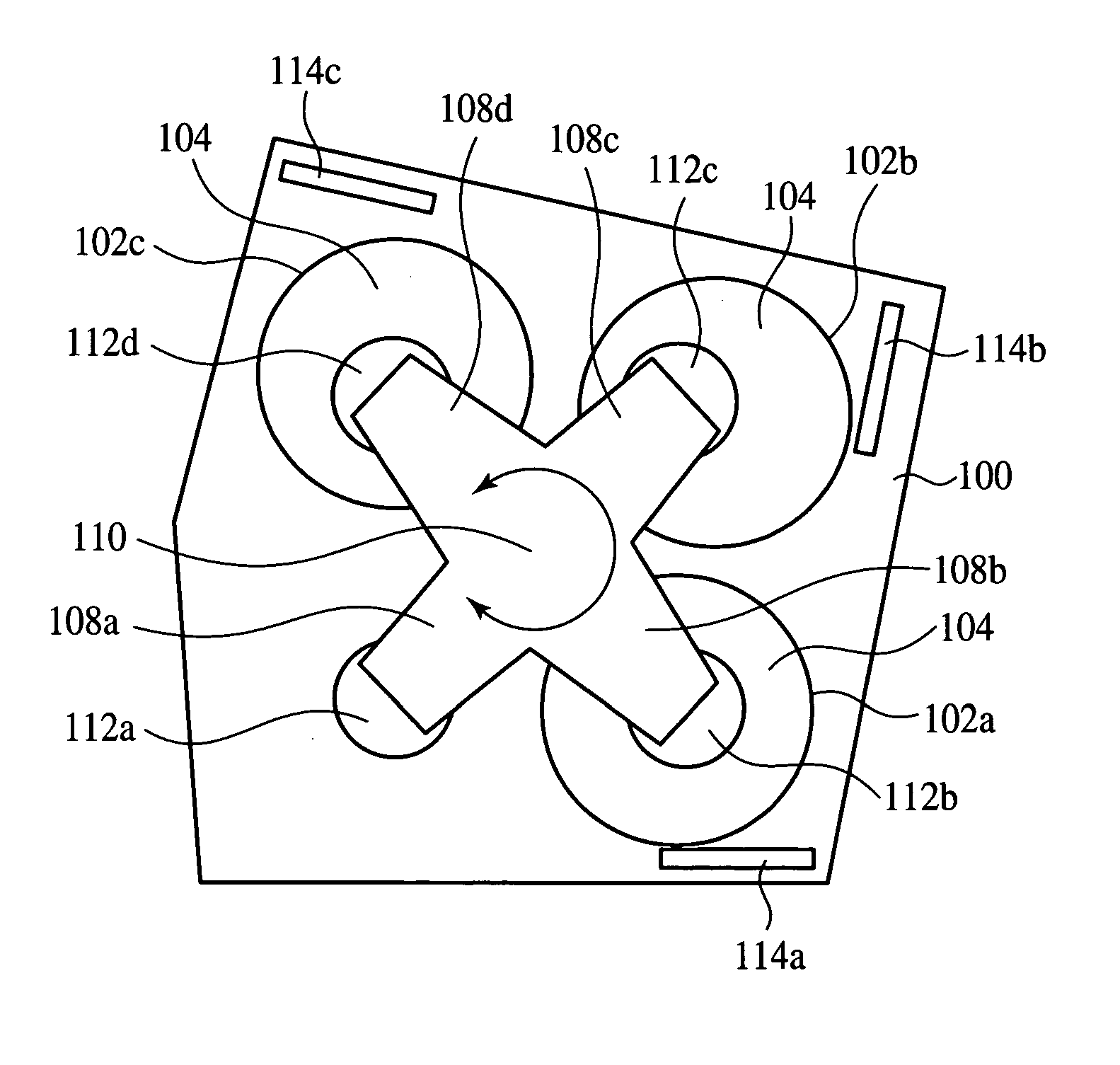
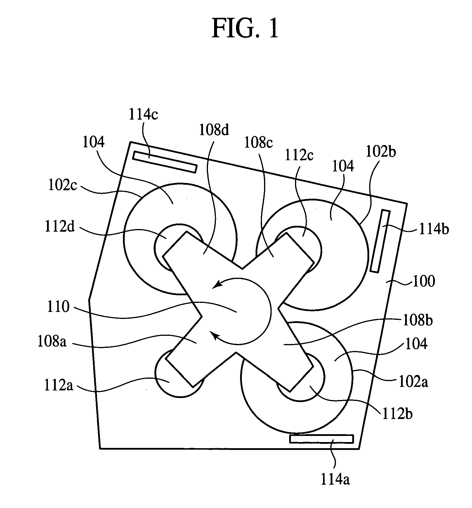
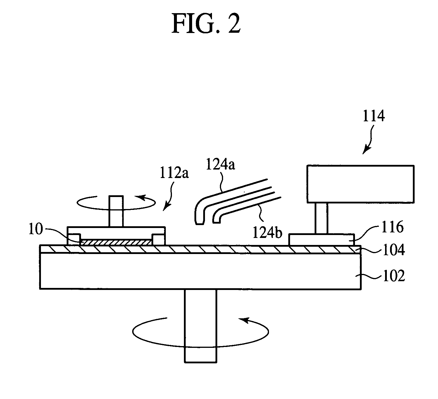
[0116] Before the semiconductor device fabrication method according to the present embodiment is explained, the polishing apparatus used in the present embodiment will be explained with reference to FIGS. 1 to 4. FIG. 1 is a plan view of the polishing apparatus. FIG. 2 is a side view of the polishing apparatus, which shows a part of the polishing apparatus shown in FIG. 1. FIG. 3 is a plan view of the polishing apparatus, which shows a part of the polishing apparatus shown in FIG. 1. FIG. 4 is an enlarged side view of the polishing apparatus, which shows a part of the polishing apparatus shown in FIG. 1.

[0117] As shown in FIG. 1, three rotary polishing tables 102a-102c are disposed on a base 100.

[0118] In the present embodiment, the polish of the surface of the film-to-be-polished is performed by, e.g., the polishing table 102a. The polishing tables 102b, 102c are usable to polish the surface of the film-to-be-polished.

[0119] As shown, polishing pads 10...

example 4

[0140] Example 4 indicates the polishing rate of the case shown in FIG. 10A where the polishing slurry is supplied to the central position P1 of the polishing pad 104, and the deionized water is supplied to the position P2 at a 12.5 cm-distance from the center of the polishing pad 104.

example 5

[0141] Example 5 indicates the polishing rate of the case shown in FIG. 10B where both the polishing slurry and the deionized water are supplied to the position P2 at a 12.5 cm-distance from the center of the polishing pad 104.

[0142] As seen in FIG. 8, the position for the polishing slurry to be supplied to and the position for the deionized water to be supplied to are changed from each other, whereby the polishing rate can be varied. Based on this, it is found that the position for the polishing slurry to be supplied to and the position for the deionized water to be supplied to are suitably set, whereby the polishing rate can be controlled.

[0143]FIG. 11 is a graph (Part 1) of intra-plane distributions of rates of polishing the films-to-be-polished with positions for the polishing slurry to be supplied to and positions for the deionized water to be supplied to suitably changed. Distances from the centers of the wafers are taken on the horizontal axis. The rates of polishing the fil...


PUM


Abstract

The method comprises the step polishing the surface of a film-to-be-polished formed over a semiconductor substrate 10 with a polishing pad while a polishing slurry containing abrasive grains, and an additive of a surfactant is being supplied onto the polishing pad 104 to thereby planarize the surface of the film-to-be-polished, and the step of further polishing the surface of the film-to-be-polished with the polishing pad while the polishing slurry and water are being supplied onto the polishing pad, after the surface of the film-to-be-polished has been planarized. In the finishing polish, not only deionized water but also the polishing slurry are supplied on to the polishing pad, a position for the polishing slurry to be supplied to and a position for the deionized water to be supplied to are suitably set, and a ratio of a supply amount of the polishing slurry and a supply amount of the deionized water is suitably set, whereby the intra-plane film thickness of the film-to-be-polished as finish-polished can be uniform.

Description

CROSS-REFERENCE TO RELATED APPLICATION [0001] This application is based upon and claims priority of Japanese Patent Application No. 2003-283810, filed on Jul. 31, 2003, and Japanese Patent Application No. 2004-13357, filed on Jan. 21, 2004, the contents being incorporated herein by reference. BACKGROUND OF THE INVENTION [0002] The present invention relates to a semiconductor device fabrication method, more specifically, a semiconductor device fabrication method in which a film-to-be-polished is polished. [0003] Conventionally, as a technique for forming device isolation regions for defining device regions, LOCOS (LOcal Oxidation of Silicon) has been widely known. [0004] However, when device isolation regions are formed by LOCOS, bird's beaks decrease the device regions. Reducing the oxidation amount for forming the device isolation regions can make the bird's beaks smaller, but when the oxidation amount is small, the device isolation function is not sufficient. When the device isola...

Claims


Application Information

Patent Timeline
Patent Type & Authority Applications(United States)
IPC IPC(8): B24B37/00B24B37/013B24B49/16H01L21/302H01L21/304H01L21/3105H01L21/321H01L21/762H01L21/768
CPCB24B37/013B24B37/042B24B49/16H01L21/7684H01L21/3212H01L21/76229H01L21/76819H01L21/31053
Inventor WATANABE, TAKASHIIDANI, NAOKIISOME, TOSHIYUKI
Owner FUJITSU SEMICON LTD
Why Eureka
Try Eureka