Semiconductor device and an electronic device

a technology of semiconductor devices and electronic devices, applied in semiconductor devices, semiconductor/solid-state device details, electrical apparatus, etc., can solve the problems of large noise produced in the power terminal of the output circuit, the scale of the circuit formed on one semiconductor chip increases, and the increase in the number of external terminals becomes insignificant, so as to reduce the number of external power terminals, suppress power noise, and scale down

Inactive Publication Date: 2005-02-10
RENESAS ELECTRONICS CORP
View PDF2 Cites 13 Cited by
  • Summary
  • Abstract
  • Description
  • Claims
  • Application Information

AI Technical Summary

Benefits of technology

[0008] An object of the present invention is to provide a semiconductor device which reduces the number of external power terminals while suppressing power noise. Another object of the present invention is to provide a semiconductor device which realize its scale down while suppressing power noise. A further object of the present invention is to provide an electronic device efficiently equipped with a bypass condenser. The above, other objects and novel features of the present invention will become apparent from the description of the present specification and the accompanying drawings.

Problems solved by technology

It is known that when an output circuit for causing such a large current to flow is provided, large noise is produced in a power terminal of the output circuit.
With advances in micro-fabrication of a device, however, the scale of a circuit formed on one semiconductor chip increases and correspondingly the number of external terminals has a tendency to increase.
The increase in the number of the external terminals becomes insignificant so far owing to the micro-fabrication or the like of the device on the semiconductor chip side.
However, a package substrate equipped therewith needs to use one large in size in association with the increase in the number of the external terminals, so that the cost of the package substrate increases and the size of a semiconductor device per se also increases, thus causing a problem that becomes the factor that interferes with downsizing of an electronic device.

Method used


Image

  • Semiconductor device and an electronic device
  • Semiconductor device and an electronic device
  • Semiconductor device and an electronic device

Examples


Embodiment Construction

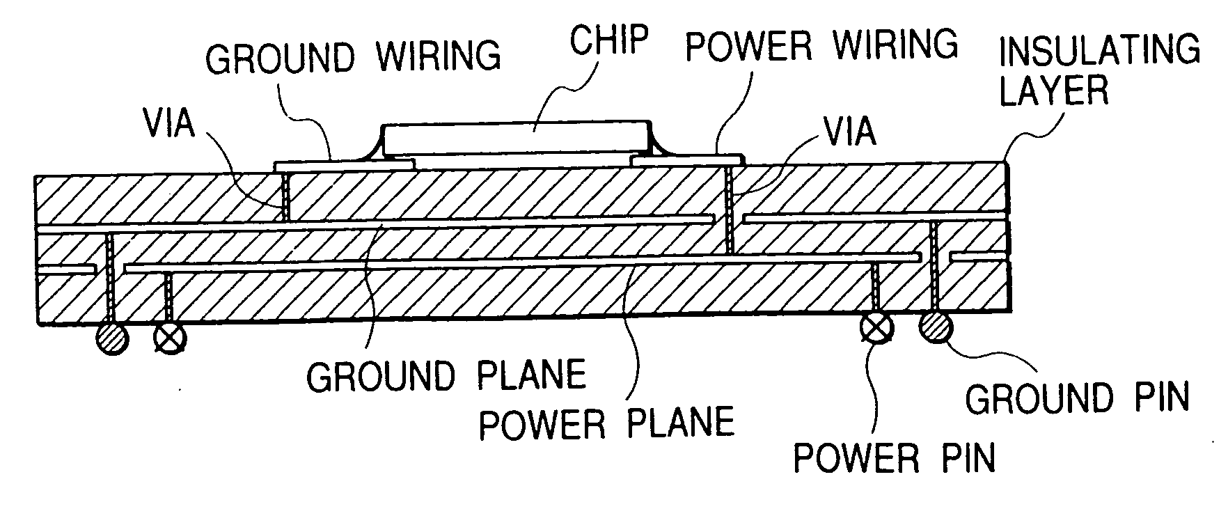
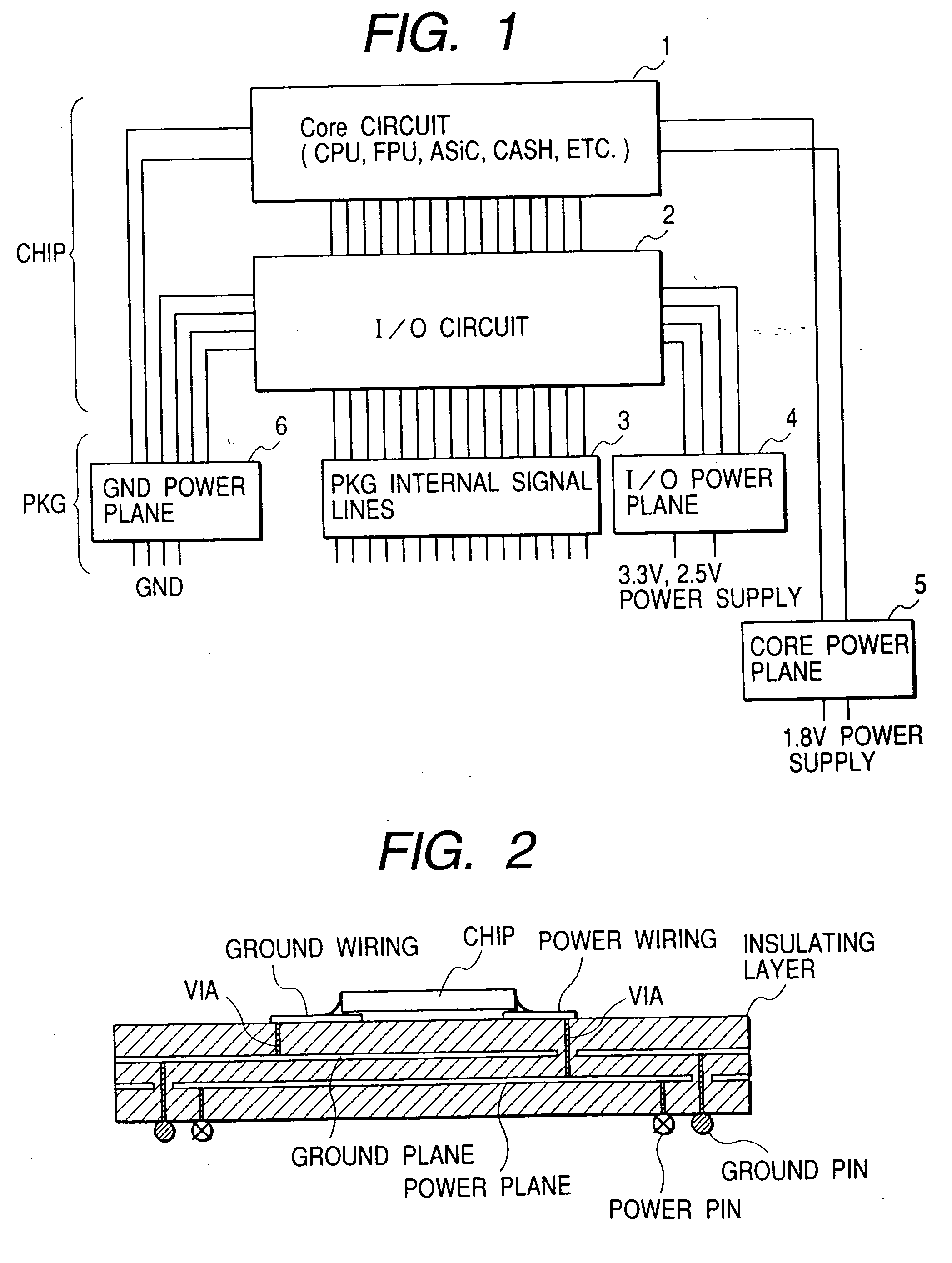
[0045] A block diagram of one embodiment of a semiconductor device according to the present invention is shown in FIG. 1. The semiconductor device showing the present embodiment is intended for a flip-chip type BGA package. The present block diagram is different from a block diagram of a general semiconductor device. A wiring unit of a PKF (Package) section is also shown together in addition to an electronic circuit constituted of a semiconductor chip section.

[0046] The semiconductor chip section comprises a core circuit 1, and an I / O circuit 2. The core circuit 1 constitutes an internal circuit and is made up of a logical circuit or the like. While the I / O circuit 2 means an input / output circuit in general, the I / O circuit 2 employed in the present embodiment indicates an output circuit.

[0047] The PKG section comprises PKG internal signal lines 3 for connecting between the I / O circuit 2 and external terminals, and a power supply system for supplying operating voltages to the inte...


PUM


Abstract

A semiconductor device has a reduced number of external power terminals and is scaled down while suppressing power noise, and an electronic device is efficiently equipped with a bypass condenser. A package substrate has, on its surface, a semiconductor chip having a plurality of output circuits and at least one electrode for supplying a voltage to each of the output circuits, and is provided with external terminals on its back surface and has a plurality of wiring layers.

Description

BACKGROUND OF THE INVENTION [0001] The present invention relates to a semiconductor device and an electronic device, and mainly to a semiconductor device having a BGA (Ball Grid Array) structure and a technology effective for application to a power supply technique of an electronic device equipped with the semiconductor device. [0002] It has been reported that Unexamined Patent Publication No. Hei 9(1997)-22977 (hereinafter called Reference 1) and Unexamined Patent Publication No. Hei 11(1999)-324886 (hereinafter called Reference 2) exist as ones considered to be those related to the invention of the present application as a result of investigations of the known examples subsequent to the completion of the invention of the present application. Reference 1 has proposed a BGA structure wherein signal pads, ground pads and power pads are alternately disposed and wires are made substantially parallel and approximately identical in length to thereby reduce noise or the like. Power and gr...

Claims


Application Information

Patent Timeline
Patent Type & Authority Applications(United States)
IPC IPC(8): H01L23/12H01L23/48H01L23/498H01L23/50H01L23/52H01L27/04H01L31/0336
CPCH01L23/49822H01L2224/73265H01L23/50H01L2224/48227H01L2924/15173H01L2924/15174H01L2924/15192H01L2924/15311H01L2924/15312H01L2924/19041H01L2924/19106H01L2924/30107H01L2924/3011H01L24/48H01L2224/16225H01L2224/32225H01L2224/73204H01L2924/13091H01L23/49838H01L2224/16235H01L2924/00H01L2924/00012H01L24/73H01L2224/05599H01L2224/45099H01L2224/85399H01L2924/00014H01L2924/14H01L2924/181H01L2224/45015H01L2924/207H01L27/04
Inventor SUWA, MOTOOMABUCHI, YUICHINAKAMURA, ATSUSHIFUKUMOTO, HIDESHI
Owner RENESAS ELECTRONICS CORP
Why Eureka
Try Eureka