Field effect transistor fabrication including formation of a channel in a pore

a field effect transistor and pore technology, applied in the field of field effect transistors, can solve the problems of difficult to control absolute dimensions and tolerances at the level of 100 nm or less by conventional lithography processes, distances between the heavily doped regions of nanowires, and relatively small siz

Inactive Publication Date: 2005-02-10
HEWLETT PACKARD DEV CO LP
View PDF4 Cites 33 Cited by
  • Summary
  • Abstract
  • Description
  • Claims
  • Application Information

AI Technical Summary

Benefits of technology

[0007] The preceding and other shortcomings of the prior art are addressed by the present invention that provides, in a first aspect, a field effect transistor. Such transistor includes a substrate having a substantially-planar upper

Problems solved by technology

Unfortunately, it has been found to be relatively difficult to control absolute dimensions and tolerances at the level of 100 nm or less by conventional lithography processes.
In many proposed devices, for example, the distances be

Method used


Image

  • Field effect transistor fabrication including formation of a channel in a pore
  • Field effect transistor fabrication including formation of a channel in a pore
  • Field effect transistor fabrication including formation of a channel in a pore

Examples


Embodiment Construction

[0024] The present invention provides a field effect transistor in silicon nanowires in which the distance between the heavily doped regions and the moderately-doped active channel region of the device is well-controlled to thereby overcome problems associated with devices formed by conventional photolithography. This is obtained by a device configuration in which the distance between the highly-doped source and drain regions and a gate electrode is carefully controlled by controlling the thicknesses of deposited layers of material rather than through reliance upon the processes of photolithography to define such regions.

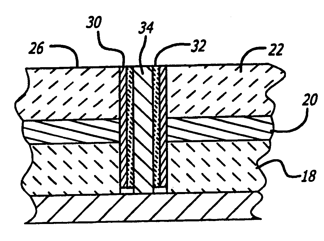
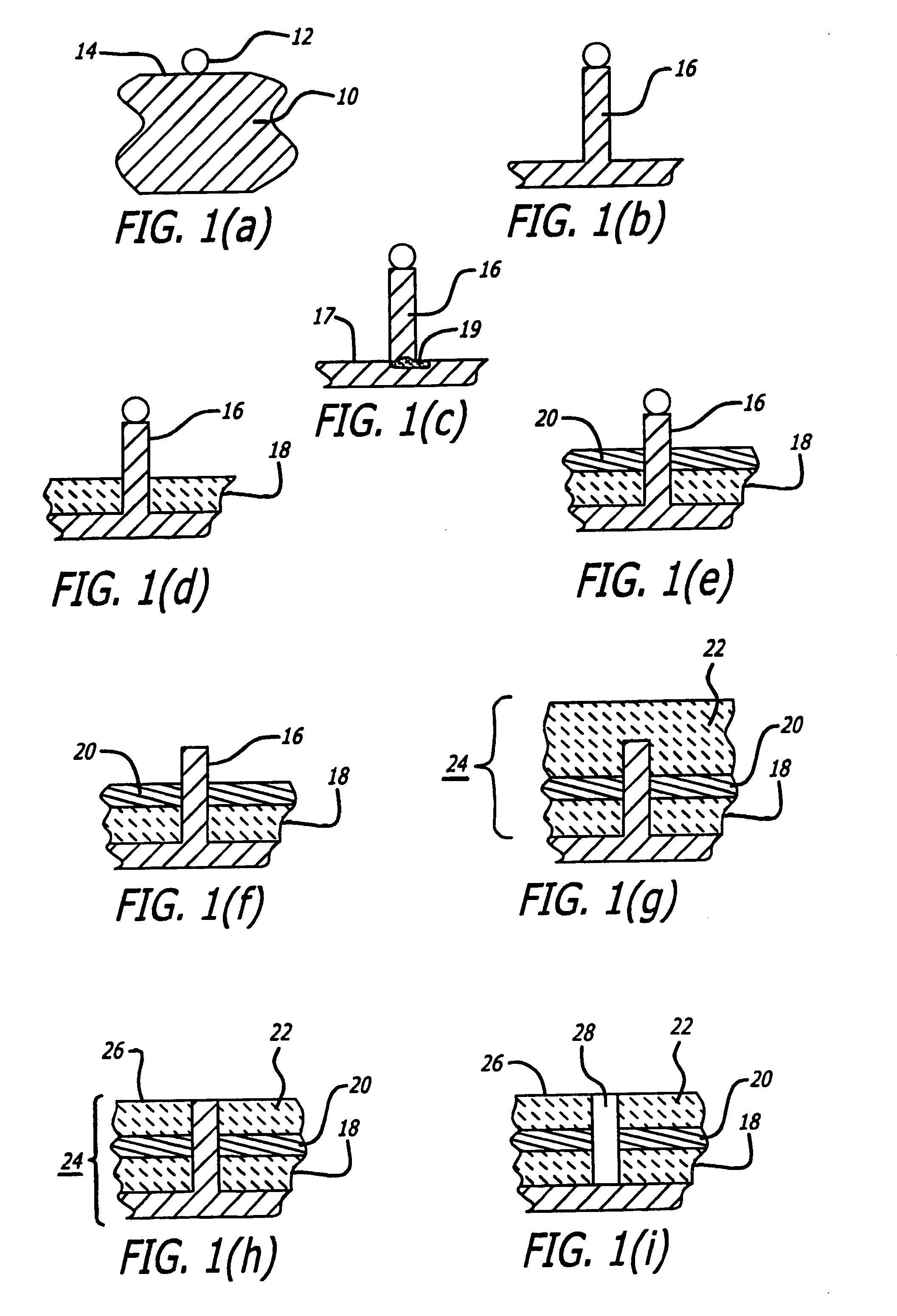
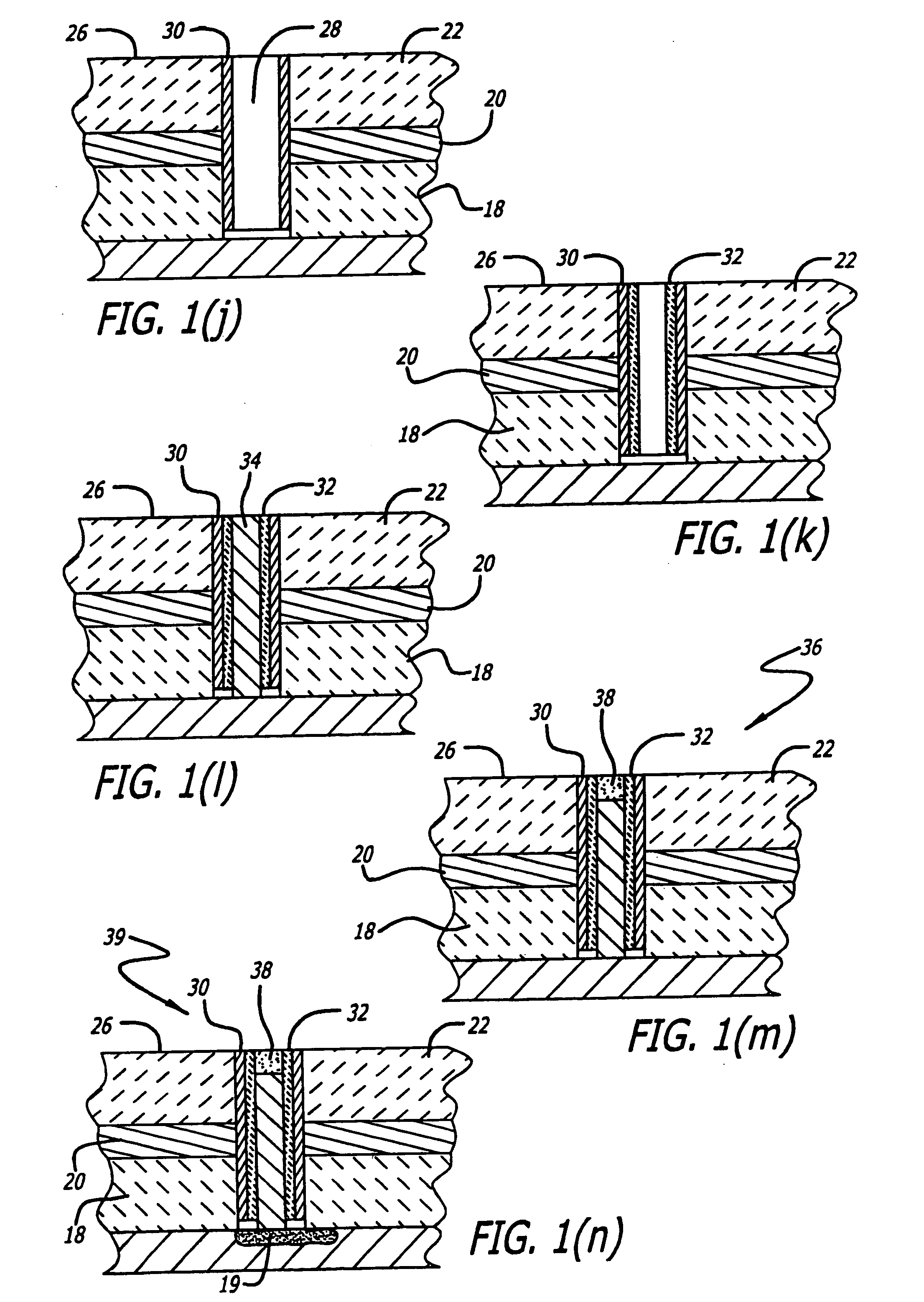
[0025] FIGS. 1(a) through 1(n) are a series of cross-sectional views that illustrate resultant structures formed during a process for making a FET in accordance with an embodiment of the invention. The process is begun by providing a substrate 10. The substrate 10 may be of either a (globally or locally) highly-doped single crystal semiconductor or a single crystal...


PUM


Abstract

A field effect transistor having a narrow channel and a method for forming such a device. An upstanding nanopillar is formed from a substrate by directional etching of the substrate preferentially masked by a nanoparticle. A stack of planar layers of material is formed adjacent and around the nanopillar. The bottom layer, adjacent the substantially planar top substrate surface, comprises insulating material. A conductive gate layer overlies the bottom layer while a second insulating layer overlies the gate layer. The pillar material is etched to leave a nanopore into which semiconductor material is deposited, forming an upstanding channel, after insulating material has been deposited on the interior of the nanopore. The source or drain may be a conductive substrate or a doped region of the substrate formed immediately beneath the nanopillar with the other electrode formed by doping the region adjacent the top of the channel.

Description

BACKGROUND [0001] 1. Field of the Invention [0002] The present invention relates to field effect transistors (FETs). More particularly, this invention pertains to a field effect transistor having an elongated conductive channel that is inclined with respect to the upper surface of an etched substrate. [0003] 2. Description of the Prior Art [0004] Many proposals have been made for making field effect transistors in silicon nanowires. Elongated nanowires of silicon are characterized by diameters on the order of 5 to 30 nanometers, substantially smaller than conventional integrated circuits that include devices having corresponding dimensions on the order of 100 nanometers or more. [0005] Efficient modulation of the conductance of the channel region of a nanowire FET requires that the channel region of the nanowire be only moderately doped while the regions external to the active channel (source and drain) should be heavily doped to reduce series resistance. (Generally, a “heavily dope...

Claims


Application Information

Patent Timeline
IPC IPC(8): H01L21/336H01L29/786
CPCH01L29/0673H01L29/0676H01L29/78696H01L29/6675H01L29/78642H01L29/66742
Inventor KAMINS, THEODORE I.
Owner HEWLETT PACKARD DEV CO LP
Why Eureka
Try Eureka