System and method for determining the temperature of a semiconductor wafer

a technology of semiconductor wafers and temperature determination methods, applied in the direction of semiconductor/solid-state device testing/measurement, baking oven, drying machines, etc., can solve the problems of affecting and causing damage to the supporting surface. , to achieve the effect of good thermal coupling, high degree of operation convenience, and favorable to the accuracy of temperature determination

Inactive Publication Date: 2005-02-24
POLARIS INNOVATIONS LTD
View PDF15 Cites 316 Cited by
  • Summary
  • Abstract
  • Description
  • Claims
  • Application Information

AI Technical Summary

Benefits of technology

[0011] The present invention provides a method with the aid of which the temperature of a semiconductor wafer can be determined with a high degree of accuracy at the time of thermal contact of the semiconductor wafer with a temperature sensing element.
[0012] In one embodiment of the invention, there is a method for determining the temperature of a semiconductor wafer at the time of thermal contact of the semiconductor wafer with a temperature sensing element in which a temperature profile of the temperature sensing element is recorded from the time of thermal contact of the semiconductor wafer with the temperature sensing element up to the time of thermal equilibrium between the semiconductor wafer and the temperature sensing element. Subsequently, the temperature of the semiconductor wafer at the time of thermal contact of the semiconductor wafer with the temperature sensing element is determined on the basis of a time period between the time of thermal contact and the time of thermal equilibrium of the semiconductor wafer and the temperature sensing element and the temperature of the semiconductor wafer reached at the time of thermal equilibrium of the semiconductor wafer and the temperature sensing element is determined by back calculation with the aid of an equation derived from Newton's law of cooling. If the parameters entered in this equation are known, this method makes it possible to determine with a high degree of accuracy the temperature of the semiconductor wafer at the time of thermal contact of the semiconductor wafer with the temperature sensing element.
[0013] The time of thermal equilibrium between the semiconductor wafer and the temperature sensing element is preferably determined on the basis of a zero point of the derivative with respect to time of the recorded temperature profile of the temperature sensing element. This zero point corresponds to the time of first thermal equilibrium between the semiconductor wafer and the temperature sensing element, since the temperature profile of the temperature sensing element is characterized by an increase as from the time of thermal contact, by a transit through a maximum at the time of first thermal equilibrium and by a subsequent decrease in the thermal equilibrium corresponding to the temperature of the semiconductor wafer. On the one hand, this allows short measuring times to be achieved, on the other hand the method is simplified, since such a determination of the thermal equilibrium can be carried out independently or automatically by corresponding measuring devices or evaluation devices.
[0014] In order to automate the method according to the invention further, the time of thermal contact of the semiconductor wafer and the temperature sensing element is preferably equated with a time of a temperature increase in the temperature profile of the temperature sensing element. This allows the recording of the temperature profile by the temperature sensing element to be triggered by an increase in the temperature of the temperature sensing element, which can be realized very easily, for example with the aid of a triggering element that is sensitive to temperature changes.
[0016] The temperature determining device preferably has a triggering element, which triggers the recording of the temperature profile by the temperature sensing element as soon as the temperature of the temperature sensing element increases. Such a temperature determining device provides a high degree of operating convenience.
[0017] In still another embodiment of the invention, there is a receiving device for a semiconductor wafer with such a temperature determining device, the temperature determining element of which is arranged on a supporting surface of the receiving device that is designed for bearing the semiconductor wafer. The arrangement of the temperature sensing element on the supporting surface produces good thermal coupling between the semiconductor wafer and the temperature sensing element, which is conducive to the accuracy of the determination of the temperature of the semiconductor wafer at the time of thermal contact of the semiconductor wafer with the temperature sensing element.

Problems solved by technology

However, it is problematical that a semiconductor wafer that is removed from a production installation, and in some cases is at a high temperature, may damage a supporting surface, generally consisting of plastic, when it is deposited into a FOUP box.
This is also the case in particular whenever process-related problems in a production installation cause an excessive temperature of a semiconductor wafer, and damage to the supporting surface is consequently brought about.
Similar problems may also occur on supporting surfaces in cooling chambers for example.
Process-related problems in the production installations that cause excessive temperatures of the semiconductor wafers can also be sensed.
However, it is disadvantageous that the temperature at the time when a semiconductor wafer is deposited on a supporting surface, that is the temperature at the time when there is first thermal contact of the semiconductor wafer with a thermocouple, cannot be determined directly, since only the temperature of the thermocouple itself is measured and, in the case of ambient temperature, this is below the temperature of the semiconductor wafer at this time.
However, in this time period the semiconductor wafer is already cooling down, so that the elapsed time period leads to a measuring error, which corresponds to the difference between the temperature of the semiconductor wafer at the time of thermal contact and at the time of thermal equilibrium.
Such a measuring error occurs even under optimum conditions, i.e. when there is a relatively great thermal capacity of the semiconductor wafer with respect to the thermocouple and when there is good thermal contact between the semiconductor wafer and the thermocouple, since a certain time period always elapses before the thermocouple is in thermal equilibrium with the semiconductor wafer.
However, the problem here is that different thermal couplings between the semiconductor wafer and the thermocouple lead to different correction values, but there is generally insufficient time to check the thermal coupling for each measurement in order to make approximately constant measuring conditions possible, and consequently to use constant correction values.
It is also problematical to maintain the fixed time period exactly, so that measuring inaccuracies may in turn arise.

Method used


Image

  • System and method for determining the temperature of a semiconductor wafer
  • System and method for determining the temperature of a semiconductor wafer
  • System and method for determining the temperature of a semiconductor wafer

Examples


first embodiment

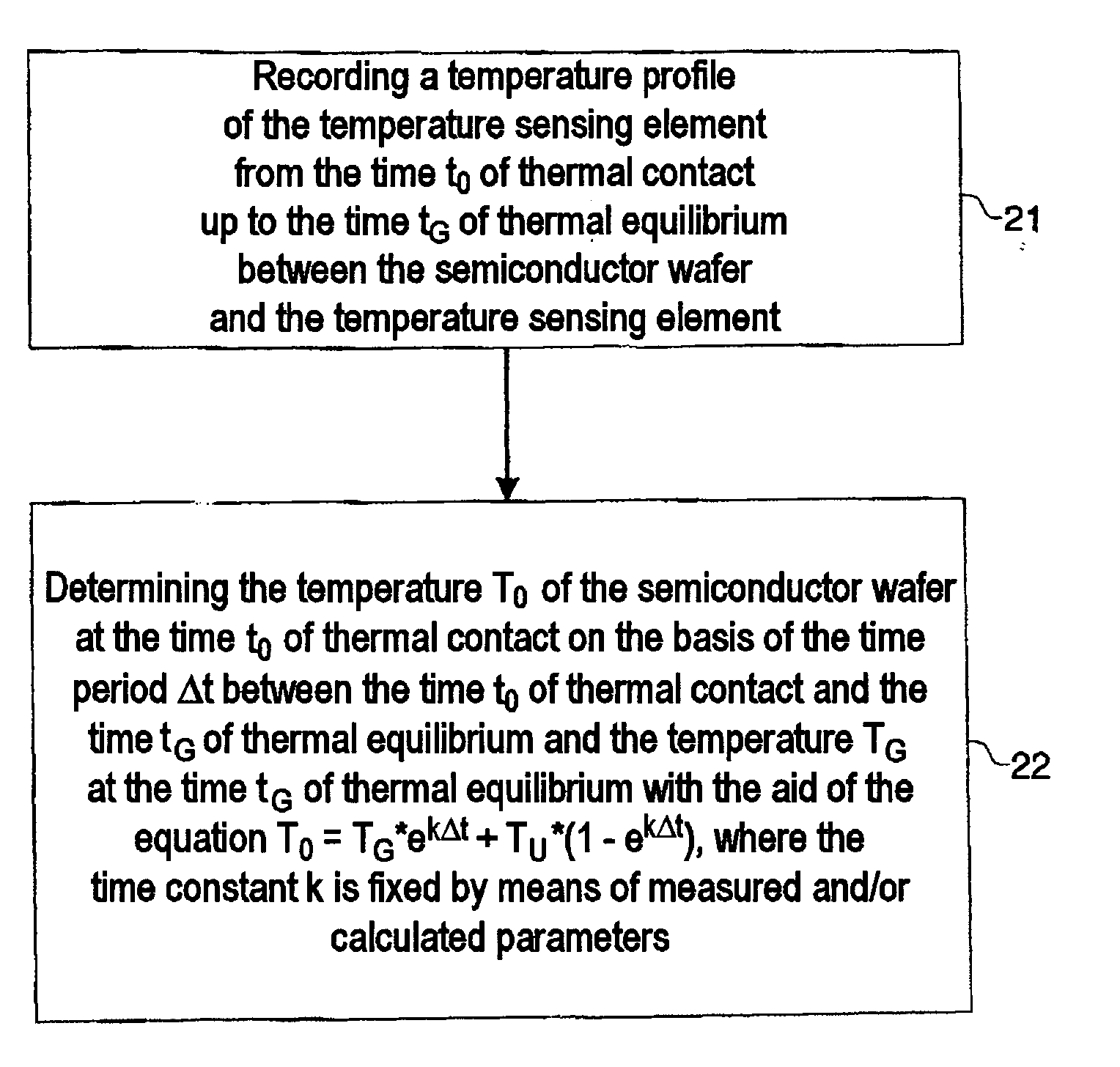
[0024]FIG. 1 shows a flow diagram of a method according to the invention for determining the temperature T0 of a semiconductor wafer at the time t0 of thermal contact of the semiconductor wafer with a temperature sensing element, the temperature T0 of the semiconductor wafer at this time t0 lying above the temperature of the temperature sensing element, which is at an ambient temperature TU.

[0025] For this purpose, in 21, a temperature profile of the temperature sensing element is recorded from the time to of thermal contact of the semiconductor wafer with the temperature sensing element up to the time tG of thermal equilibrium between the semiconductor wafer and the temperature sensing element.

[0026] Subsequently, in 22, the temperature T0 of the semiconductor wafer at the time t0 of thermal contact of the semiconductor wafer with the temperature sensing element is determined on the basis of a time period Δt between the time t0 of thermal contact and the time tG of thermal equilib...

second embodiment

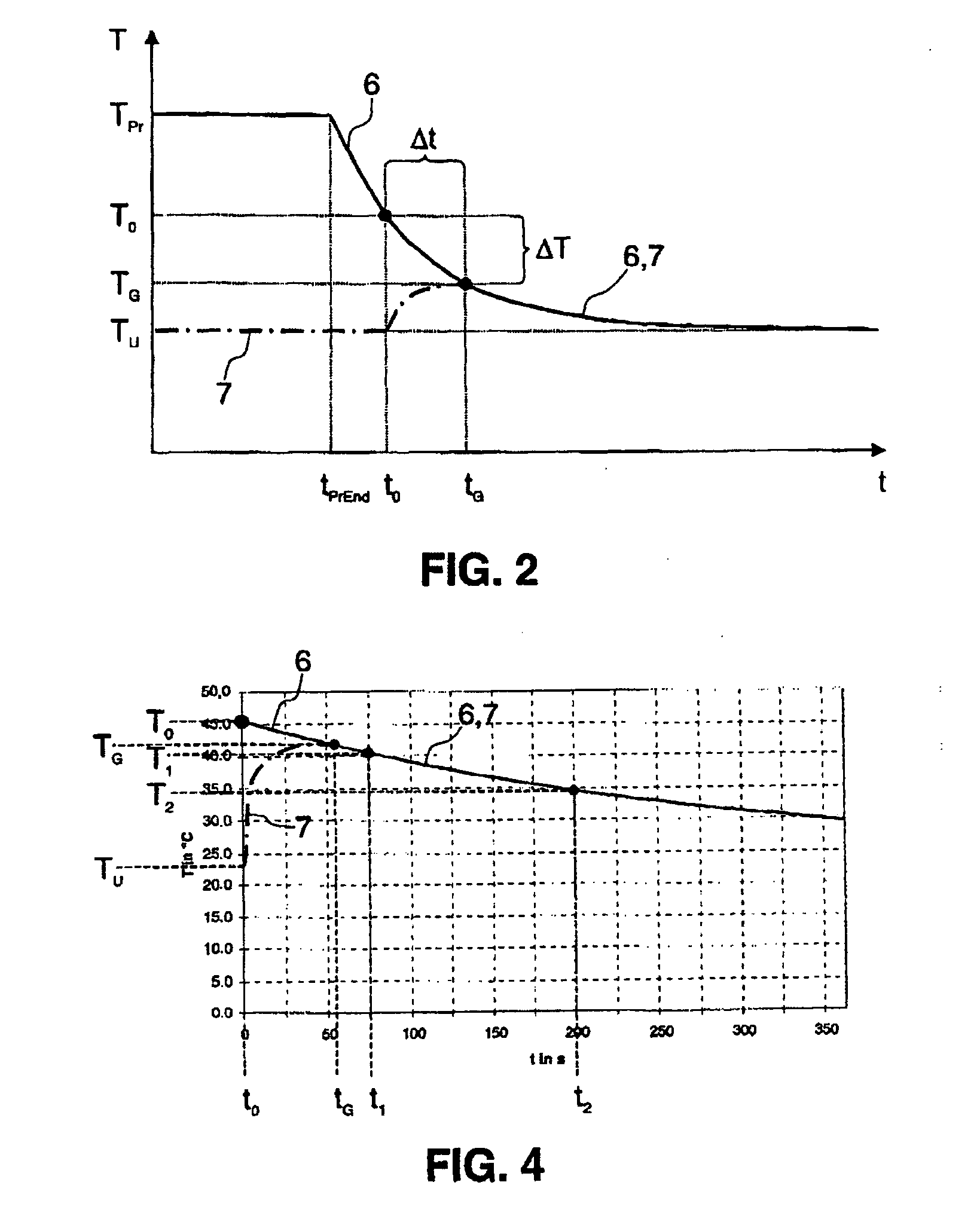
[0038] If these parameters α, A, c and m are not known or cannot be measured or this would require excessive effort, there are other possibilities for determining the value of the time constant k. In this respect, FIG. 3 shows a flow diagram of a method according to the invention for determining the temperature T0 of a semiconductor wafer at the time t0 of thermal contact of the semiconductor wafer with a temperature sensing element.

[0039] As a difference from the embodiment represented in FIG. 1, in the case of the method according to the invention that is represented in FIG. 3, in 220, the time constant k is calculated from a first temperature value T1 and a second temperature value T2, which are recorded at a first time t1 and a second time t2 as from the time tG of thermal equilibrium between the semiconductor wafer and the temperature sensing element.

[0040] This method is illustrated on the basis of the following FIG. 4, which shows a further diagram of the temperature profile...


PUM

PropertyMeasurementUnit
temperatureaaaaaaaaaa
heat transfer coefficientaaaaaaaaaa
specific heat capacityaaaaaaaaaa

Abstract

A system and method for determining the temperature of a semiconductor wafer at the time of thermal contact of the semiconductor wafer with a temperature sensing element. According to the invention, a temperature profile of the temperature sensing element is recorded from the time of thermal contact up to the time of thermal equilibrium between the semiconductor wafer and the temperature sensing element and the temperature of the semiconductor wafer at the time of thermal contact is determined on the basis of a time period between the time of thermal contact and the time of thermal equilibrium and the temperature TG of the semiconductor wafer reached at the time tG of thermal equilibrium is determined by back calculation with the aid of an equation derived from Newton's law of cooling.

Description

CLAIM FOR PRIORITY [0001] This application claims the benefit of priority to German Application No. 103 28 660.8-33, filed in the German language on Jun. 26, 2003, the contents of which are hereby incorporated by reference. TECHNICAL FIELD OF THE INVENTION [0002] The present invention relates to a system and method for determining the temperature of a semiconductor wafer at the time of thermal contact of the semiconductor wafer with a temperature sensing element. BACKGROUND OF THE INVENTION [0003] Semiconductor components today dominate a large part of electronics. These components comprise a complex arrangement of electronic structures which are interconnected to one another in a number of planes arranged one above the other on a semiconductor substrate, also referred to as a chip. The production of chips on a semiconductor slice, referred to hereafter as a semiconductor wafer, is characterized by a large number of production steps, which are carried out in different production ins...

Claims


Application Information

Patent Timeline
Patent Type & Authority Applications(United States)
IPC IPC(8): G01K7/42H01L21/66
CPCH01L22/00G01K7/42
Inventor PEUKERT, KARSTEN
Owner POLARIS INNOVATIONS LTD
Why Eureka
Try Eureka