Method and platform for integrated physical verifications and manufacturing enhancements

a technology of physical verification and manufacturing enhancement, applied in the field of circuit design, schematic verification and photomask making prior to the manufacture of integrated circuits, can solve the problems of insufficient achievement of these objects, and achieve the effect of high storage, memory and run-time efficiency

Inactive Publication Date: 2005-02-24
RPX CORP
View PDF23 Cites 105 Cited by
  • Summary
  • Abstract
  • Description
  • Claims
  • Application Information

AI Technical Summary

Benefits of technology

[0026] Another object of the present invention is to provide a system for automated physical verification and enhancement which has high storage, memory and run-time efficiency.
[0027] Yet another object of the present invention is to provide a system for automated physical verification and enhancement which has a graphical, easy-to-use and an object-oriented, script-like user interfaces.

Problems solved by technology

Evidently, it is not sufficient to achieve these objects by using a common data format or database amongst all the tools involved.

Method used


Image

  • Method and platform for integrated physical verifications and manufacturing enhancements
  • Method and platform for integrated physical verifications and manufacturing enhancements
  • Method and platform for integrated physical verifications and manufacturing enhancements

Examples


Embodiment Construction

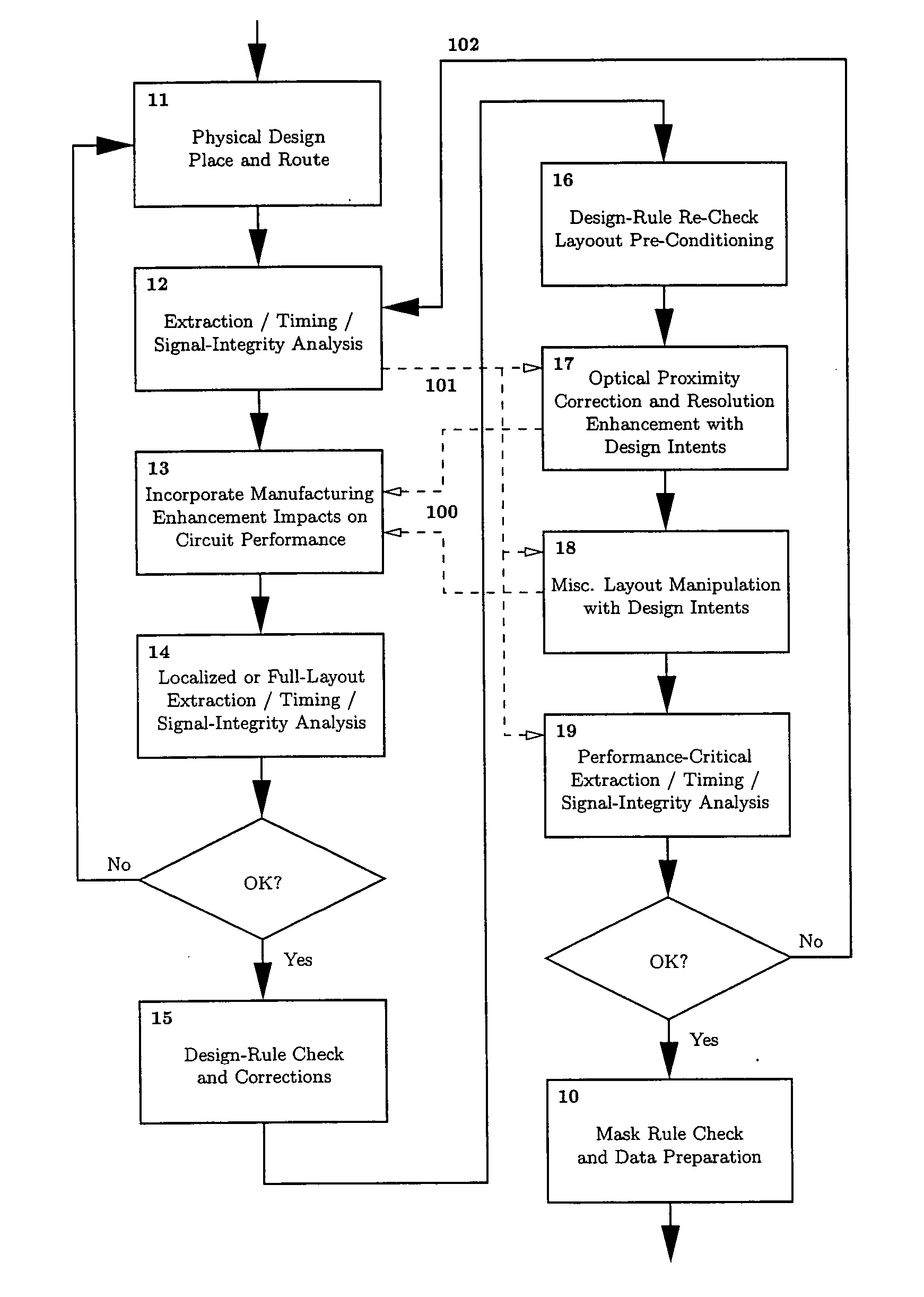
[0033] A software platform consisting of a collection of software tools functionally bound together with an underlying structure so that different tools can communicate with each other and be controlled via a unified interface to the end-user. The platform also allows the possibility of adding, modifying, removing and / or customizing its components or engines, as long as the components utilize a pre-defined set of interfaces to the platform.

[0034] A data structure that permits representations, handling and manipulations of both layout circuit connectivity and geometry patterning information. The data structure represents a set of polygons. Each polygon has a set of vertices which describe its shape and location, plus two or more pointers to link, or define an association, with other polygons. With this data structure, a layout can be “fractured” and described by a set of polygons, where the circuit connectivity are described by linking electronically-connected polygons using the so-...


PUM


Abstract

An automated design for manufacturability platform which provides integrated physical verification and manufacturing enhancement operations. The platform uses an efficient data structure capable of handling and manipulating both layout circuit and geometry characteristics, which permits a wide range of operations such as timing analysis, design-rule checking and optical proximity corrections on a single platform. This feature eliminates the need to translate layout representations between various tools without the requirement of using a common database. Moreover, the platform's common user interface enables encapsulated information exchange between the design and the manufacturing teams, permiting early consideration of manufacturing distortion or enhancement impact on circuit performance.

Description

FIELD OF INVENTION [0001] The present invention relates to circuit design, schematic verification and making of photomasks prior to manufacture of integrated circuits. More specifically, the present invention is directed to automated digital logic synthesis and placement systems and enhancements for manufacturability, yield and performance which allow the device designer and the IC manufacturer to collaborate on optimizing the circuit design, device layout and manufacturing yields prior to making of the masks. BACKGROUND OF INVENTION [0002] In the prior art, the process of designing an integrated circuit on a typical CAD system is done in several discrete steps using different software tools and data bases. Once specifications for the IC are in place, the circuit for the product is designed, typically using a synthesis tool, followed with verification of the design using logic simulation tools and formal verification tools to ensure the resulting logical representation of the circui...

Claims


Application Information

Patent Timeline
Patent Type & Authority Applications(United States)
IPC IPC(8): G06FG06F9/45G06F9/455G06F15/18G06F17/50
CPCG06F17/5081G06F30/398
Inventor WU, SHAO-POHO, TSZ-TAK DANIEL
Owner RPX CORP
Why Eureka
Try Eureka