Photocathode having A1GaN layer with specified Mg content concentration

a photocathode and content concentration technology, applied in the field of semiconductor photocathodes, can solve the problem that the quantum efficiency of conventional semiconductor cathodes cannot be described as sufficient, and achieve the effect of high quantum efficiency and high quantum efficiency

Inactive Publication Date: 2005-03-03
HAMAMATSU PHOTONICS KK
View PDF5 Cites 3 Cited by
  • Summary
  • Abstract
  • Description
  • Claims
  • Application Information

AI Technical Summary

Benefits of technology

[0003] However, when an attempt is made to perform precise measurements, the quantum efficiency of such conventional semiconductor cathodes cannot be described as sufficient, and AlxGa1-xN system semiconductor photocathodes with still higher quantum efficiencies are desired. The present invention is intended to resolve this problem, and has as an object the provision of a semiconductor photocathode with high quantum efficiency, having an optical absorption layer formed from AlxGa1-xN (0≦x≦1).

Problems solved by technology

However, when an attempt is made to perform precise measurements, the quantum efficiency of such conventional semiconductor cathodes cannot be described as sufficient, and AlxGa1-xN system semiconductor photocathodes with still higher quantum efficiencies are desired.

Method used


Image

  • Photocathode having A1GaN layer with specified Mg content concentration
  • Photocathode having A1GaN layer with specified Mg content concentration
  • Photocathode having A1GaN layer with specified Mg content concentration

Examples


first embodiment

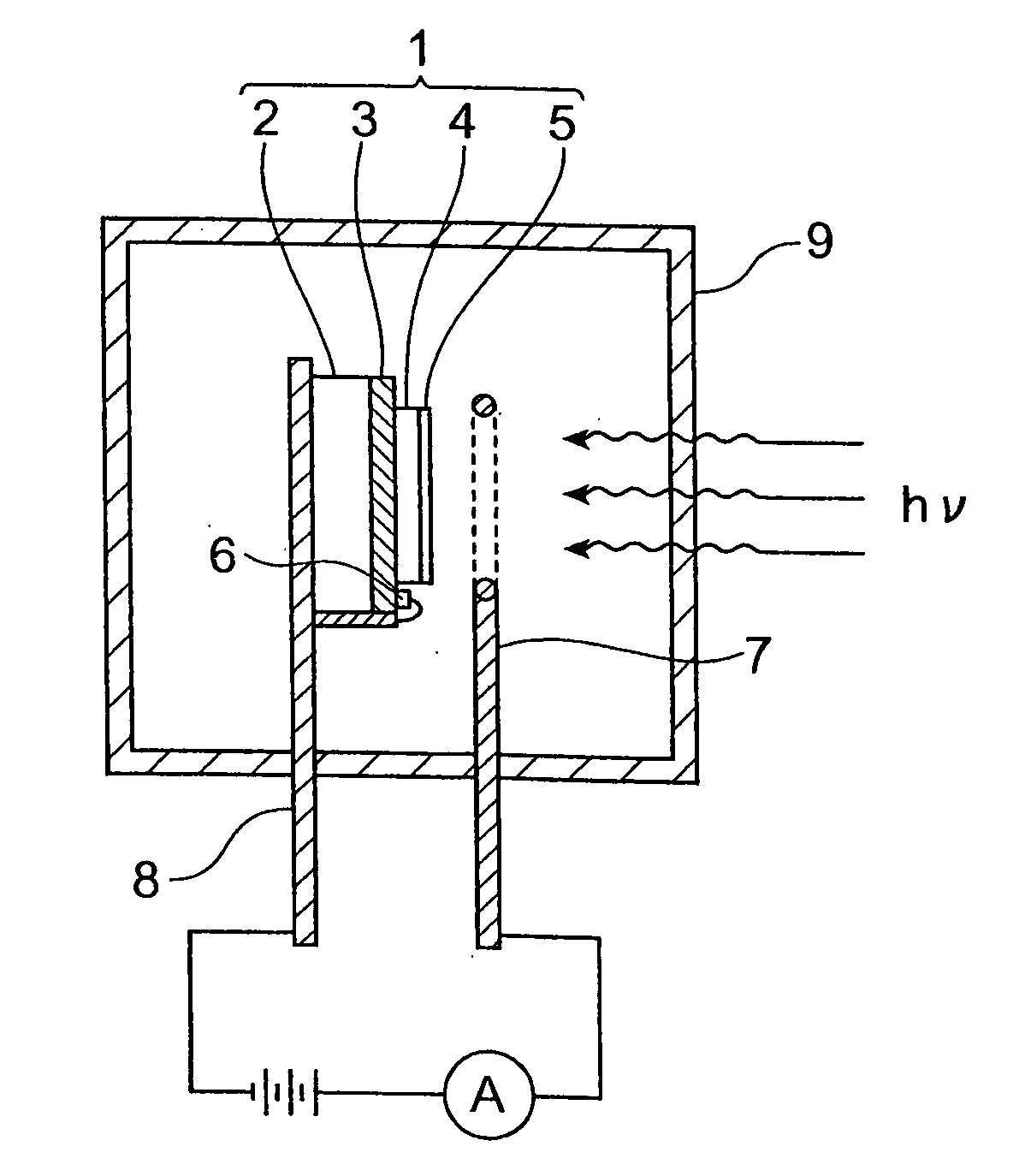
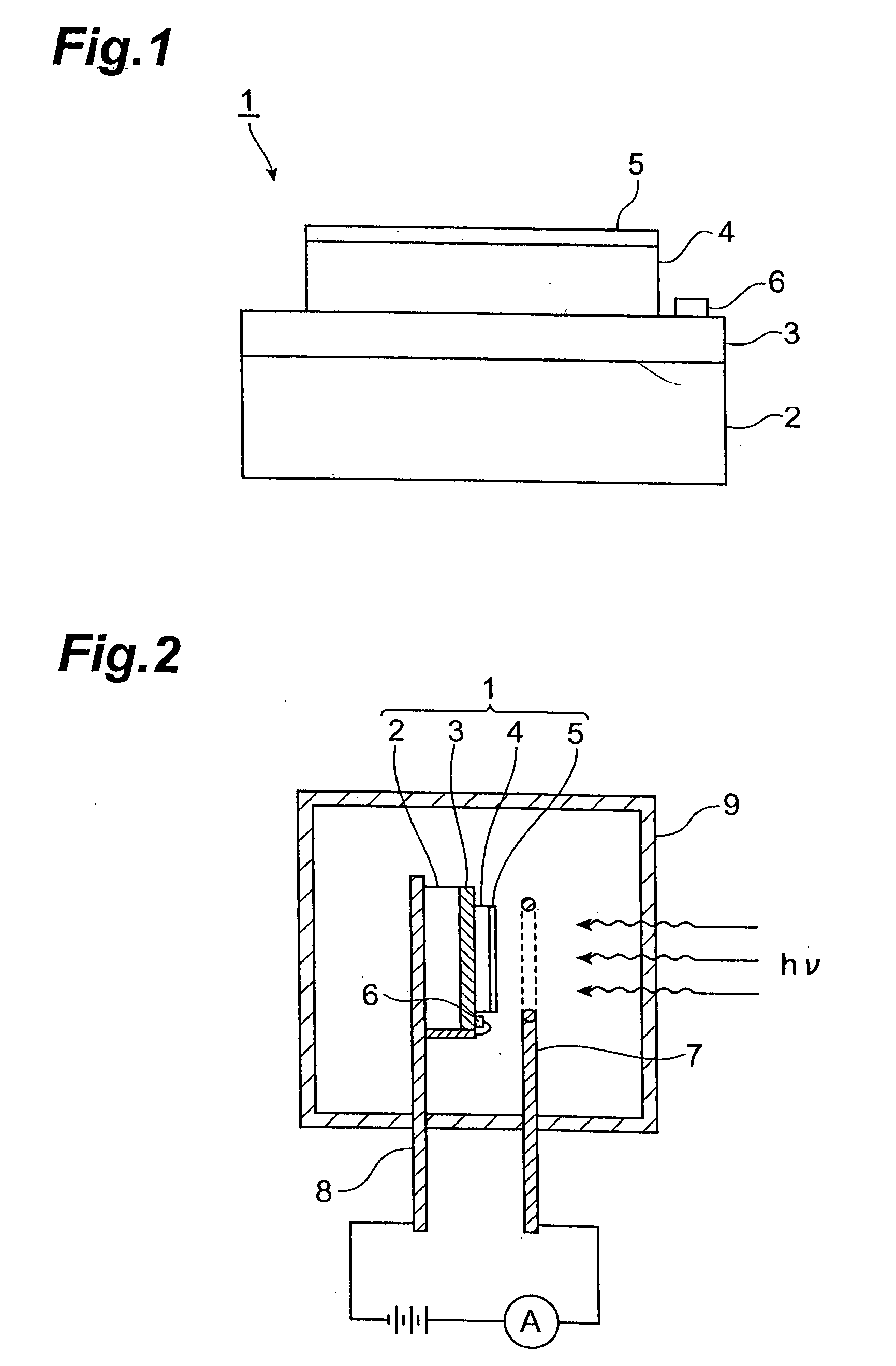
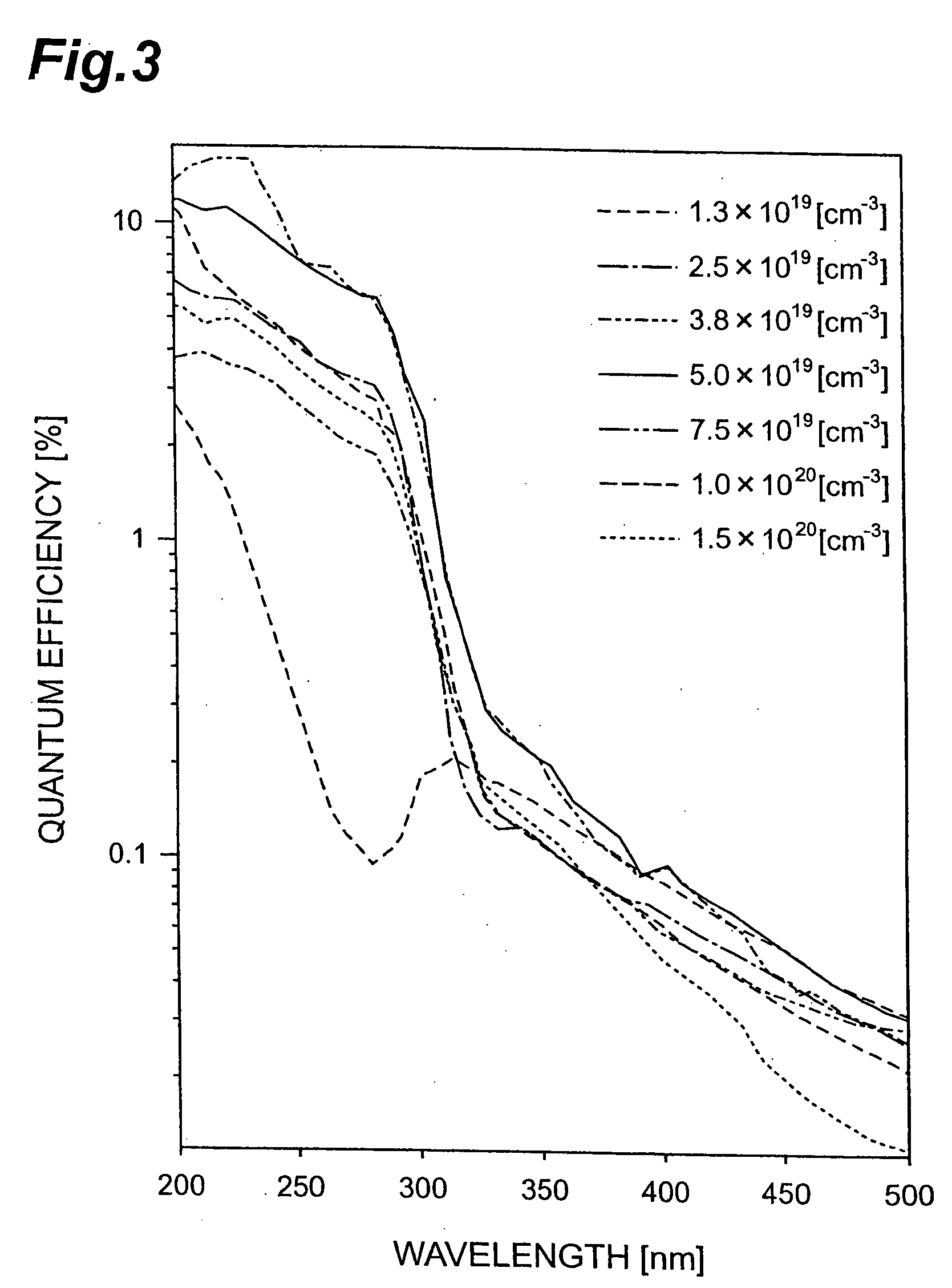
[0019]FIG. 1 is a drawing showing the structure of a reflection-type semiconductor photocathode of a first embodiment, employing an AlxGa1-xN layer (0≦x≦1) as an optical absorption layer. FIG. 2 is a schematic diagram showing schematically a measurement method to measure the photoelectric characteristics of the semiconductor photocathode of FIG. 1. FIG. 3 is a characteristic diagram showing the wavelength dependence of the quantum efficiency of the semiconductor photocathode of FIG. 1. FIG. 4 is a characteristic diagram showing the Mg concentration dependence of the quantum efficiency, for light at a wavelength of 280 nm, of the semiconductor photocathode of FIG. 1. FIG. 5 is a characteristic diagram showing the Mg concentration dependence of the ratio RS / L of the quantum efficiency for light at a wavelength of 280 nm to the quantum efficiency for light at a wavelength of 200 nm, for the reflection-type semiconductor photocathode of FIG. 1.

[0020] As shown in FIG. 1, in the reflectio...

second embodiment

[0074]FIG. 7 is a characteristic diagram showing the wavelength dependence of the quantum efficiency of the transmission-type semiconductor photocathode 11 of the FIG. 7 compares the wavelength dependences of a plurality of semiconductor photocathodes, with the same configuration but with different Mg concentrations in the optical absorption layer 4. Except for the different amounts of Cp2Mg supplied, the plurality of semiconductor photocathodes 11 were fabricated by the same method described above.

[0075] As is clear from FIG. 7, at wavelengths of approximately 300 nm or below the semiconductor photocathode 11 of the second embodiment (with an Mg concentration in the optical absorption layer 4 of 5×1019 cm−3) exhibits a quantum efficiency of 2 to 4%, and exhibits satisfactory solar-blind characteristics. For light in the 200 to 280 nm wavelength range, the quantum efficiency was particularly high at approximately 4.1%.

[0076] From FIG. 7, it is seen that the quantum efficiency depe...


PUM


Abstract

Ultraviolet light incident from the side of a surface layer 5 passes through the surface layer 5 to reach an optical absorption layer 4. Light which reaches the optical absorption layer 4 is absorbed within the optical absorption layer 4, and photoelectrons are generated within the optical absorption layer 4. Photoelectrons diffuse within the optical absorption layer 4, and reach the interface between the optical absorption layer 4 and the surface layer 5. Because the energy band is curved in the vicinity of the interface between the optical absorption layer 4 and surface layer 5, the energy of the photoelectrons is larger than the electron affinity in the surface layer 5, and so photoelectrons are easily ejected to the outside. Here, the optical absorption layer 4 is formed from an Al0.3Ga0.7N layer with an Mg content concentration of not less than 2×1019 cm−3 but not more than 1×1020 cm−3, so that a solar-blind type semiconductor photocathode 1 with high quantum efficiency is obtained.

Description

TECHNICAL FIELD [0001] This invention relates to a semiconductor photocathode, formed using a semiconductor as a component material, and which is excited by incident light and emits photoelectrons. BACKGROUND ART [0002] Conventional semiconductor photocathodes for use with ultraviolet light were formed for example from AlxGa1-xN. Preexisting technology related to such semiconductor photocathodes formed from AlxGa1-xN is disclosed in the specification of U.S. Pat. No. 5,557,167, the specification of U.S. Pat. No. 4,616,248, and in Japanese Patent Laid-open No. 08-96705. Conventional semiconductor photocathodes formed from AlxGa1-xN have a quantum efficiency sufficient to enable practical application in the ultraviolet light. DISCLOSURE OF THE INVENTION [0003] However, when an attempt is made to perform precise measurements, the quantum efficiency of such conventional semiconductor cathodes cannot be described as sufficient, and AlxGa1-xN system semiconductor photocathodes with still ...

Claims


Application Information

Patent Timeline
Patent Type & Authority Applications(United States)
IPC IPC(8): H01J1/34H01J29/38H01J31/50H01J40/06H01J43/08
CPCH01J1/34H01J31/507H01J2231/50021H01J43/08H01J40/06
Inventor KAN, HIROFUMINIIGAKI, MINORUOHTA, MASASHITAKAGI, YASUFUMIUCHIYAMA, SHOICHI
Owner HAMAMATSU PHOTONICS KK
Why Eureka
Try Eureka