Light receiving device circuit-built-in type light receiving unit and optical disk unit

a light receiving unit and circuit-built-in technology, applied in the direction of basic electric elements, semiconductor devices, electrical appliances, etc., can solve the problems of poor production yield and higher cost of conventional light receiving devices, inability to read data from disks, and leakage current between light receiving parts to allow light receiving devices to function properly. , to achieve the effect of excellent sensitivity

Inactive Publication Date: 2005-03-03
SHARP KK
View PDF6 Cites 3 Cited by
  • Summary
  • Abstract
  • Description
  • Claims
  • Application Information

AI Technical Summary

Benefits of technology

[0012] According to the above configuration, three or more-layer translucent films are disposed on the light receiving parts and on the part between the plurality of the light receiving parts in the light receiving device, and materials of the adjacent translucent films are different from each other, so that two or more interfaces are formed between these three or more-layer translucent films. Electrons or holes produced, for example, during a production process, are distributed and stored in the above-stated two or more interfaces. Conventionally, the electrons and the holes are stored in one interface between two-layer translucent films. Therefore, the light receiving device of the present invention is smaller in intensity of electric fields that are formed in the light receiving parts and in the part between the light receiving parts by the stored electrons or holes than the conventional light receiving device. As a result, inversion of a conductive type is reduced in the part between the plurality of the light receiving parts. Therefore, current hardly flows in the part between the plurality of the light receiving parts, and therefore leak current between the light receiving parts is effectively controlled.
[0033] According to the above configuration, the light receiving device or the circuit-built-in type light receiving unit that is almost free from leak current and has excellent sensitivity is provided, which makes it possible to provide an optical disk unit suitable for read and write access to a high-density storage optical disk with use of, for example, a blue laser.

Problems solved by technology

However, there is a problem that the conventional device is susceptible to leak current between a plurality of the light receiving parts, and at worst, leak current between the light receiving parts becomes too large for the light receiving device to function properly.
The problem is attributed to holes stored in an interface between the silicon oxide and the silicon nitride forming the antireflection structure.
Therefore, the conventional light receiving device has poor production yield and higher costs, which poses a problem of inadequacy as an optical disk unit.
Further, in the conventional light receiving device, if the surface of the antireflection structure is exposed to air, the silicon nitride on the surface of the antireflection structure gradually oxidizes and therefore a reflectance of the antireflection structure is changed.
This leads to a problem of inappropriate read of data from a disk.
The above problems become more notable as incident light to the light receiving device has longer wavelength.
According to these reasons, the conventional light receiving device suffers rapid oxidation of the surface layer of the antireflection structure upon reception of short-wavelength light, and so the reflectance on the surface of the antireflection structure is drastically changed by the oxidation, by which the power of light reaching the light receiving parts is significantly changed from the power of incident light, causing drastic change in signal outputs.
Therefore, there is a problem that the conventional light receiving device is not adequate for receiving short-wavelength light.

Method used


Image

  • Light receiving device circuit-built-in type light receiving unit and optical disk unit
  • Light receiving device circuit-built-in type light receiving unit and optical disk unit
  • Light receiving device circuit-built-in type light receiving unit and optical disk unit

Examples


first embodiment

[0045]

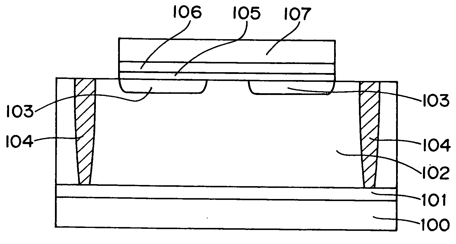
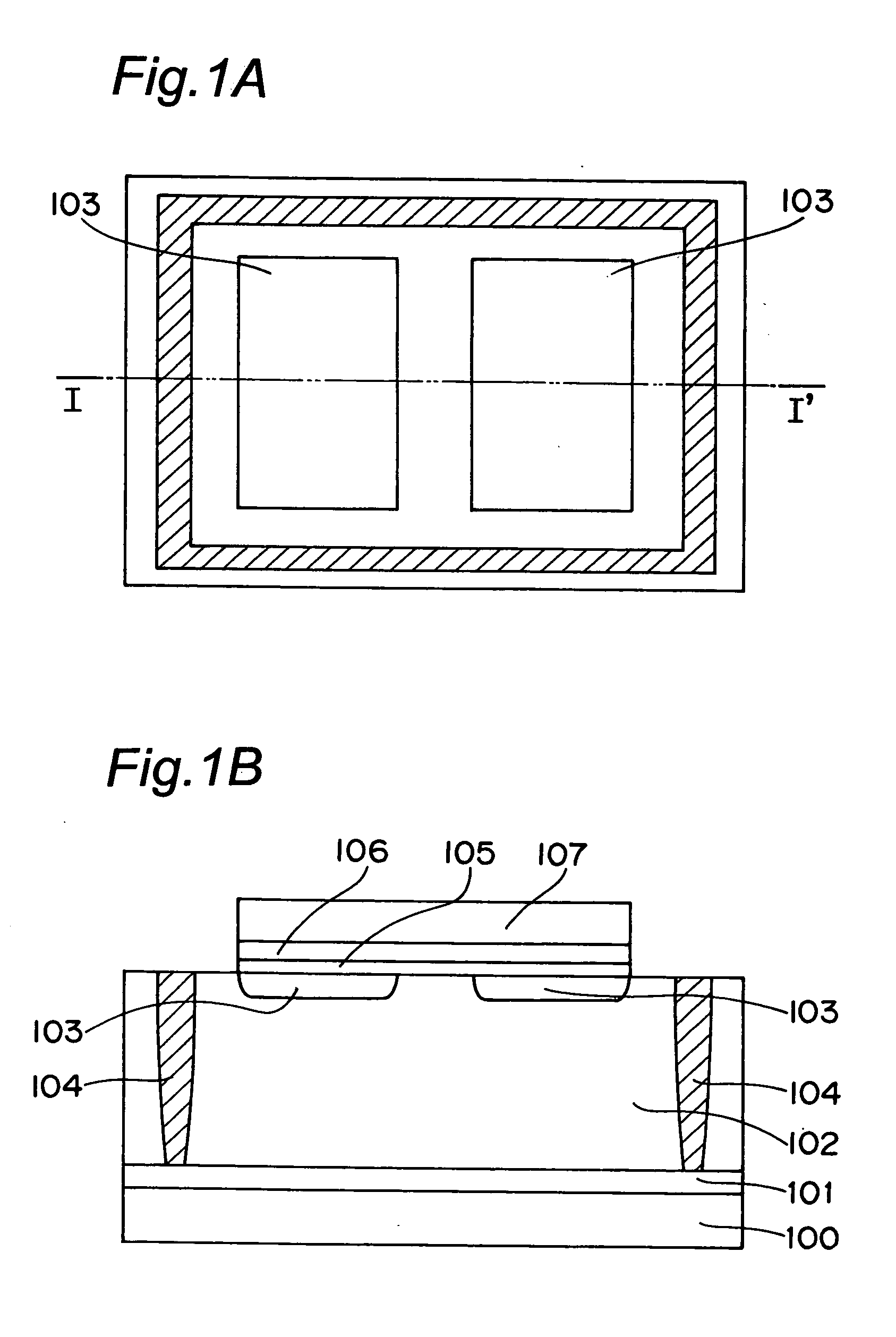
[0046]FIG. 1A is a plan view showing a light receiving device in a first embodiment of the present invention, while FIG. 1B is a cross sectional view of FIG. 1A taken on the line I-I′. In FIGS. 1A and 1B, contacts, metal interconnections, and interlayer insulating films formed after a contact step are deleted. In FIG. 1A, a first silicon oxide 105, a silicon nitride 106 and a second silicon oxide 107 are deleted.

[0047] The light receiving device comprises a first P-type diffusion layer 101 with impurity concentration of about 1E18 cm−3 and a thickness of about 1 μm, and a P-type semiconductor layer 102 with a thickness of about 10 μm to 20 μm and impurity concentration of about 1E13 to 1E16 cm−3 on a silicon substrate 100. In a surface part of the P-type semiconductor layer 102, two N-type diffusion layers 103, 103 with impurity concentration of about 1E17 to 1E20 cm−3 are disposed to constitute two light receiving parts. In the N-type diffusion layers 103, any element such a...

second embodiment

[0058]

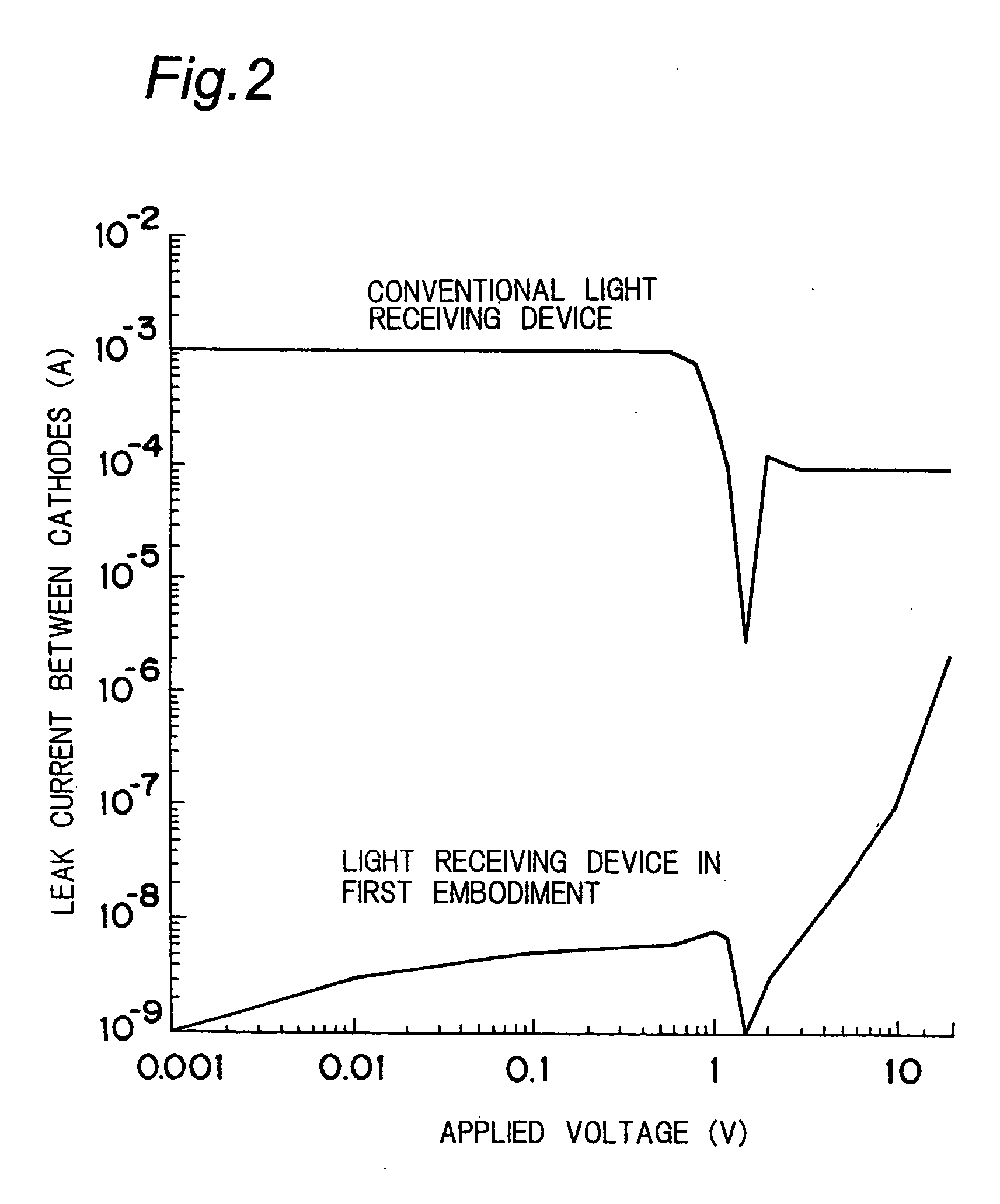
[0059]FIG. 3 is a cross sectional view showing a light receiving device in a second embodiment of the present invention. In FIG. 3, component members having the same functions as the light receiving device in the first embodiment of FIG. 1B are designated by the same reference numerals and detailed description is deleted.

[0060] As shown in FIG. 3, the light receiving device in the present embodiment is different from the light receiving device in the first embodiment only in the point that on the N-type diffusion layers 103, 103 becoming light receiving parts and on the P-type semiconductor layer 102 between these two N-type diffusion layers 103, 103, four-layer translucent films are formed and a molding resin 204 is disposed on the translucent films.

[0061] The four-layer translucent films are composed of a first silicon oxide 200 with a film thickness of about 9 nm, a first silicon nitride 201 with a film thickness of about 39 nm, a second silicon oxide 202 with a film thic...

third embodiment

[0064]

[0065]FIG. 4 is a cross sectional view showing a light receiving device in a third embodiment of the present invention. In the present embodiment, contacts, metal interconnections, interlayer insulating films and the like formed after a contact step are deleted in description.

[0066] The light receiving device comprises a P-type diffusion layer 11 with impurity concentration of about 1E18 cm−3 and a thickness of about 1 μm on a silicon substrate 10, and a P-type semiconductor 12 with impurity concentration of about 1E13 to 1E16 cm−3 and a thickness of about 10 μm to 20 μm on the P-type diffusion layer 11. On a surface part of the P-type semiconductor 12, an N-type diffusion layer 13 with impurity concentration of 1E17 to 1E20 cm−3 in the vicinity of the surface is provided, and a PN junction formed by the N-type diffusion layer 13 and the P-type semiconductor 12 constitutes a light receiving part. It is to be noted that an impurity forming the N-type diffusion layer 13 may be ...


PUM


Abstract

A first P-type diffusion layer and a P-type semiconductor layer are provided on a silicon substrate, and two N-type diffusion layers are provided on a front surface of this P-type semiconductor layer to form two light receiving units. Three-layer translucent films, a first silicon oxide film, a silicon nitride film, and a second silicon oxide film are disposed on the N-type diffusion layers and on the P-type semiconductor layer between the two diffusion layers. Holes produced during a production process and distributed and captured in two interfaces between the three-layer translucent films can reduce a field intensity in the vicinity of the surface of the P-type semiconductor layer to below a conventional level and an inversion of a conductive type to reduce a leak current between the light receiving units accordingly.

Description

[0001] This nonprovisional application claims priority under 35 U.S.C. §119(a) on Patent Applications No(s). P2001-368402 filed in Japan on Dec. 3, 2001 and P2002-003371 filed in Japan on Jan. 10, 2002, the entire contents of which are hereby incorporated by reference. TECHNICAL FIELD [0002] The present invention relates to a light receiving device, a circuit-built-in type light receiving unit and an optical disk unit. BACKGROUND ART [0003] Conventionally, an optical pickup unit for use in optical disk units is structured such that a laser light beam emitted from a semiconductor laser is split into a plurality of laser light beams by a diffraction grating, and a plurality of the laser light beams are collected by an object lens on a plurality of positions on an optical disk, and a plurality of light beams reflected and modulated on the optical disk are received by a light receiving device. The light receiving device, which has a plurality of light receiving parts formed on one semic...

Claims


Application Information

Patent Timeline
Patent Type & Authority Applications(United States)
IPC IPC(8): H01L31/0216H01L31/103
CPCH01L31/02161H01L31/1035H01L31/103H01L31/10H01L31/101
Inventor MORIOKA, TATSUYAHAYASHIDA, SHIGEKITANI, YOSHIHIKOOHKUBO, ISAMUWADA, HIDEO
Owner SHARP KK
Why Eureka
Try Eureka