
Inorganic thin layer, organic electroluminescence device including the same, and fabrication method thereof

Active Publication Date: 2005-03-03
KOREA INST OF SCI & TECH
View PDF1 Cites 22 Cited by
  • Summary
  • Abstract
  • Description
  • Claims
  • Application Information

AI Technical Summary

Benefits of technology

[0008] Therefore, an object of the present invention is to provide an inorganic thin layer which is composed of an inorganic composite containing at least two kinds of inorganic materials at a predetermined ratio and shows excellent moisture and oxygen proof.
[0009] Another object of the present invention is to provide an organic electroluminescence device which has high performance and stability, by using the inorganic thin layer as a passivation layer.
[0012] In accordance with the present invention, for example, when an inorganic thin layer is formed by using SiO2 and MgO as base materials and mixing and depositing the other inorganic materials, an oxygen transmission rate (OTR) and a water vapor transmission rate (WVTR) can be reduced more than when the inorganic thin layer is formed only by using the base materials. In addition, when an inorganic composite is deposited, an organic layer is not damaged because of a low deposition temperature.
[0024] The inorganic mono-layer or the inorganic multi-layer are barrier layers having barrier characteristics to moisture and oxygen, which can be applied to the top, the bottom or both the top and bottom of the substrate irresistible to moisture, oxygen or heat. For example, the inorganic mono-layer or the inorganic multi-layer are applied to the top, the bottom or both the top and bottom of a flexible substrate irresistible to moisture and heat such as plastic, for remarkably reducing the WVTR and the OTR.
[0027] In general, a transition temperature Tg of an organic material of the organic electroluminescence device ranges from 80 to 120° C. The organic material may be damaged over 120° C. Preferably, the inorganic thin film layer is formed by depositing the inorganic composite at a temperature below 120° C. so that physical properties of the inorganic thin film layer can be improved and the organic materials in the organic electroluminescence device can be protected.

Problems solved by technology

However, the encapsulation method is very complicated and not applied to a large area and flexible display.
However, a process for depositing SiO2 and SixNy requires a high temperature, and thus due to crystallization of the organic layers of the OLED.
In the case that an inorganic thin layer such as SiO2 and MgO is formed by using a general vacuum evaporator, it is difficult to completely implement physical properties of the material itself.
Accordingly, even though the inorganic thin layer is formed as the passivation layer of the OLED, it is not efficiently operated due to a high oxygen transmission rate (OTR) and a high water vapor transmission rate

Method used


Image

  • Inorganic thin layer, organic electroluminescence device including the same, and fabrication method thereof
  • Inorganic thin layer, organic electroluminescence device including the same, and fabrication method thereof
  • Inorganic thin layer, organic electroluminescence device including the same, and fabrication method thereof

Examples


Embodiment Construction

[0049] Reference will now be made in detail to the preferred embodiments of the present invention, examples of which are illustrated in the accompanying drawings.

[0050] An inorganic thin layer passivation layer, an organic electroluminescence device including the same, and a fabrication method thereof in accordance with the preferred embodiments of the present invention will now be described in detail with reference to the accompanying drawings. These drawings or embodiments are not intended to be limiting, but explaining the present invention.

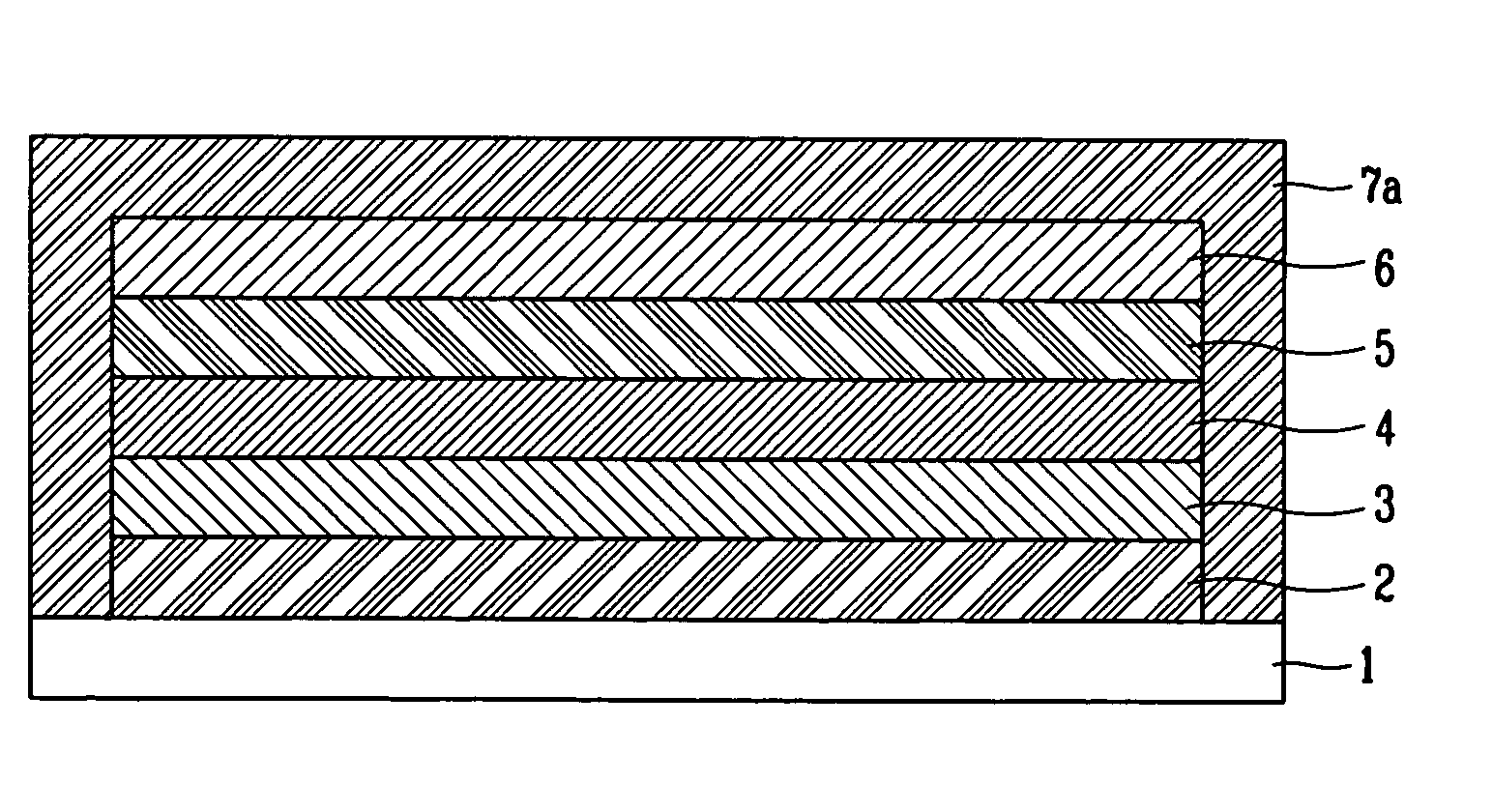
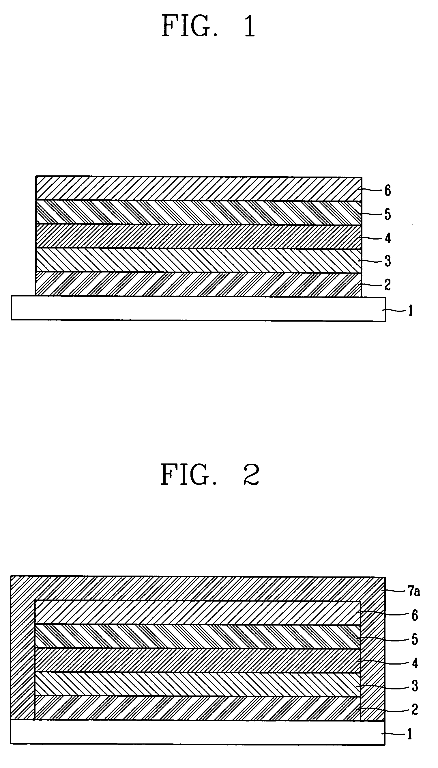
[0051]FIG. 1 is a cross-sectional diagram illustrating a general organic electroluminescence device. An ITO is deposited on a glass or plastic substrate 1 by RF-sputtering, and patterned to form an anode electrode 2. An organic layer comprised of a hole injection layer 3, a hole transfer layer 4, a light emitting layer and an electron transfer layer 5 is deposited on the anode electrode 2. Here, thermal evaporation can be used. AlLi alloy ha...


PUM


Abstract

The present invention discloses an inorganic thin layer which is composed of an inorganic composite containing at least two kinds of inorganic materials and shows excellent moisture and oxygen proof, an organic electroluminescence device including the inorganic thin layer as a passivation layer, and a fabrication method thereof.

Description

BACKGROUND OF THE INVENTION [0001] 1. Field of the Invention [0002] The present invention relates to an inorganic thin film layer which is composed of an inorganic composite containing at least two kinds of inorganic materials and shows excellent moisture and oxygen barriers, an organic electroluminescence device including the inorganic thin layer as a passivation layer, and a fabrication method thereof. [0003] 2. Description of the Background Art [0004] An Organic Light-emitting Diodes (OLEDs) are a self light emitting type, not a light receiving type like a thin film transistor-liquid crystal display (TFT-LCD). The OLED is advantageous in a response time, power consumption and brightness. Therefore, the OLED has been considered as a flat panel display replacing a liquid crystal display (LCD). The OLED is classified into a transparent OLED (TOLED), a flexible OLED (FOLED), a stacked OLED (SOLED), and a microcavity OLED (MOLED) according to functions, and into a passive mode OLED (P...

Claims


Application Information

Patent Timeline
IPC IPC(8): H05B33/14H01L51/52H05B33/00
CPCH01L24/10H01L51/5237H01L24/13H01L2224/13099H01L2924/01011H01L2924/01012H01L2924/01013H01L2924/0102H01L2924/01022H01L2924/0104H01L2924/01061H01L2924/01073H01L2924/01006H01L2924/01021H01L2924/01033H01L2924/12041H01L2924/00H01L2924/12044H01L2224/13H10K50/8445H05B33/14H10K50/844
Inventor JU, BYEONG-KWONKIM, JAI-KYEONGKIM, YOUNG-CHULKIM, HOONKIM, KWANG-HOLEE, JOO-WON
Owner KOREA INST OF SCI & TECH
Features
  • Generate Ideas
  • Intellectual Property
  • Life Sciences
  • Materials
  • Tech Scout
  • Unparalleled Data Quality
  • Higher Quality Content
  • 60% Fewer Hallucinations
Learn More