

Synchronous clock generation circuit capable of ensuring wide lock-in range and attaining lower jitter
a synchronous clock and lock-in range technology, applied in the direction of oscillation generators, pulse generation by logic circuits, generating/distributing signals, etc., can solve the problems of narrow capture range of analog pll circuits using such a vco, poor phase noise characteristic of analog phase comparators, and disadvantageous narrow capture range of analog pll circuits , to achieve the effect of wide lock-in range and excellent jitter characteristics
- Summary
- Abstract
- Description
- Claims
- Application Information
AI Technical Summary
Benefits of technology
Problems solved by technology
Method used
Image

Examples
embodiment 1
[0039] [Embodiment 1]
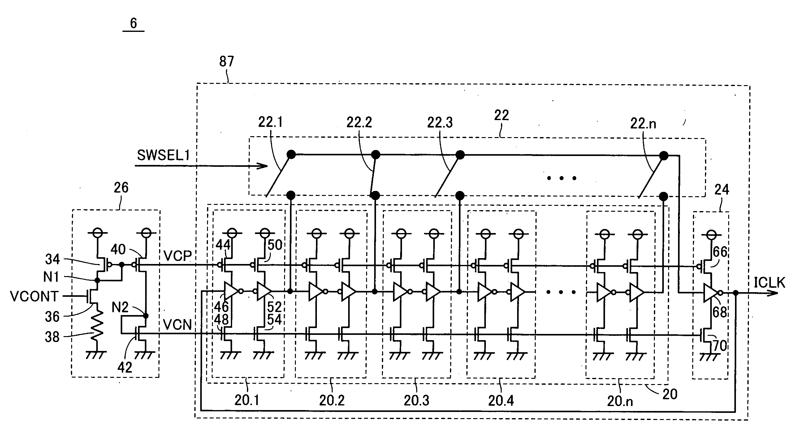
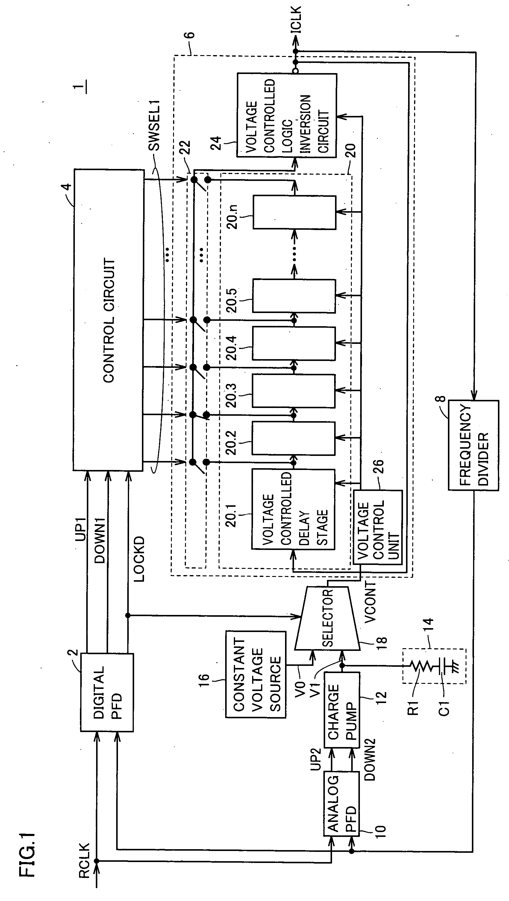
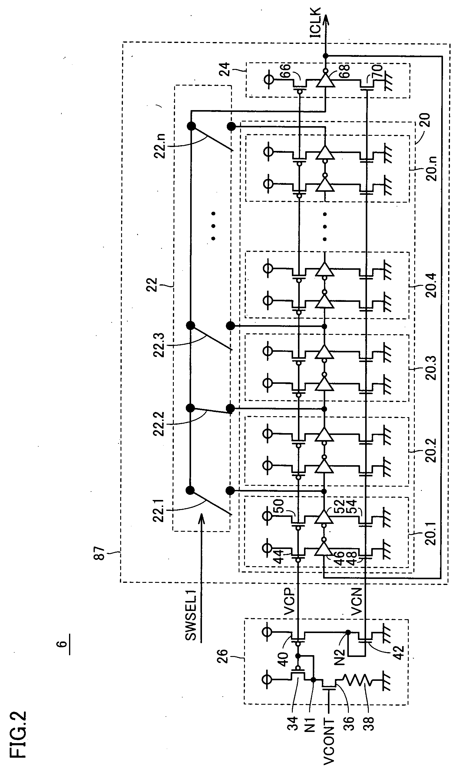
[0040]FIG. 1 is a circuit diagram showing a configuration of a synchronous clock generation circuit 1 in Embodiment 1.
[0041] Referring to FIG. 1, synchronous clock generation circuit 1 includes a frequency divider 8 dividing a frequency of a clock signal ICLK used in the chip; a digital PFD (phase comparator) 2 comparing a phase of an output signal from frequency divider 8 with a phase of an externally provided reference clock signal RCLK and outputting control signals UP1, DOWN1 and LOCKD; a control circuit 4 adjusting a frequency by varying a control signal SWSEL1 in accordance with control signals UP1, DOWN1, and fixing control signal SWSEL1 so as to maintain a current frequency when control signal LOCKD is activated; and an oscillation circuit 6 having an oscillation frequency varied in a discrete manner in accordance with control signal SWSEL1. When a control voltage VCONT varies, the oscillation frequency of oscillation circuit 6 continuously varies.
[004...
embodiment 2
[0066] [Embodiment 2]
[0067] In Embodiment 2, the synchronous clock generation circuit shown in FIG. 1 includes a control circuit 104 and an oscillation circuit 106 instead of control circuit 4 and oscillation circuit 6 respectively.
[0068]FIG. 3 is a circuit diagram showing a configuration of a control circuit and an oscillation circuit used in Embodiment 2.
[0069] Referring to FIG. 3, control circuit 104 is connected to digital PFD 2 in FIG. 1, receives control signals UP1, DOWN1 and LOCKD, and outputs a control signal SWSEL2.
[0070] Oscillation circuit 106 includes a voltage control circuit 110 outputting control voltages VCP, VCN in accordance with control voltage VCONT and control signal SWSEL2, and a ring oscillator 112 providing oscillation clock signal ICLK having an frequency varied in accordance with an output from voltage control circuit 110. Ring oscillator 112 includes five inversion delay circuits 121 to 125 connected so as to form a ring. Inversion delay circuit 125 ou...
embodiment 3
[0080] [Embodiment 3]
[0081] In the oscillation circuit in Embodiment 1, the number of delay stages has been digitally controlled while the control voltage has been controlled in an analog manner, so as to obtain a wide lock-in range and an excellent jitter characteristic. Meanwhile, in the oscillation circuit in Embodiment 2, a resistance value in the voltage control unit in the oscillation circuit has been digitally controlled, while the input control voltage has been controlled in an analog manner, so as to obtain an effect the same as in Embodiment 1. Embodiment 3 aims to achieve a similar effect by incorporating into the synchronous clock generation circuit in Embodiment 1 the oscillation circuit in which transistor sizes of the VCO are digitally controlled and the control voltage is subjected to analog control.
[0082] In Embodiment 3, synchronous clock generation circuit 1 shown in FIG. 1 includes control circuits 160 to 162 and an oscillation circuit 149 shown in FIG. 4 instea...
PUM
 Abstract
Description
Claims
Application Information