Method for developing processing and apparatus for supplying developing solution

a technology of developing processing and developing solution, which is applied in the direction of photomechanical equipment, instruments, and materials sensitive to light, can solve the problems of cd uniformity on the substrate not necessarily satisfactory, product diffused, and difficult to form satisfactory circuit patterns. , to achieve the effect of suppressing defect generation and improving cd uniformity

Inactive Publication Date: 2005-03-10
TOKYO ELECTRON LTD
View PDF13 Cites 15 Cited by
  • Summary
  • Abstract
  • Description
  • Claims
  • Application Information

AI Technical Summary

Benefits of technology

[0010] A first object of the present invention is to provide an appropriate method for a developing processing conforming to the characteristics of the resist material relative to the developing solution. A second object of the present invention is to provide a method for a developing processing with an improved CD uniformity. A third object of the present invention is to provide a me

Problems solved by technology

Under the circumstances, it is difficult nowadays to form a satisfactory circuit pattern by the conventional method for the developing processing using a developing solution of a predetermined concentration.
Therefore, in the latter stage of the developing processing, the state of equilibrium between the dissolved product remaining in a high concentration and the developing solution is collapsed, with the result that the dissolved product is diffused toward the developing solution.
In conclusion, in the conventional method for the developing processing, t

Method used


Image

  • Method for developing processing and apparatus for supplying developing solution
  • Method for developing processing and apparatus for supplying developing solution
  • Method for developing processing and apparatus for supplying developing solution

Examples


Embodiment Construction

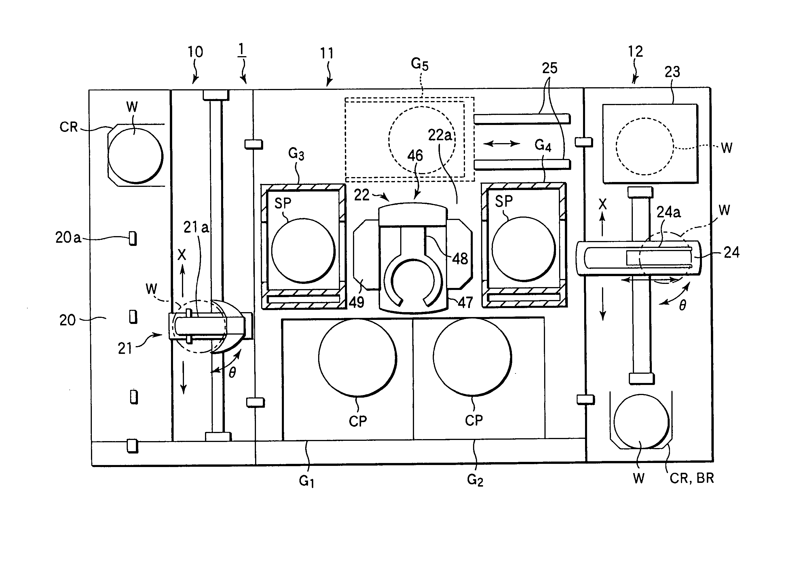
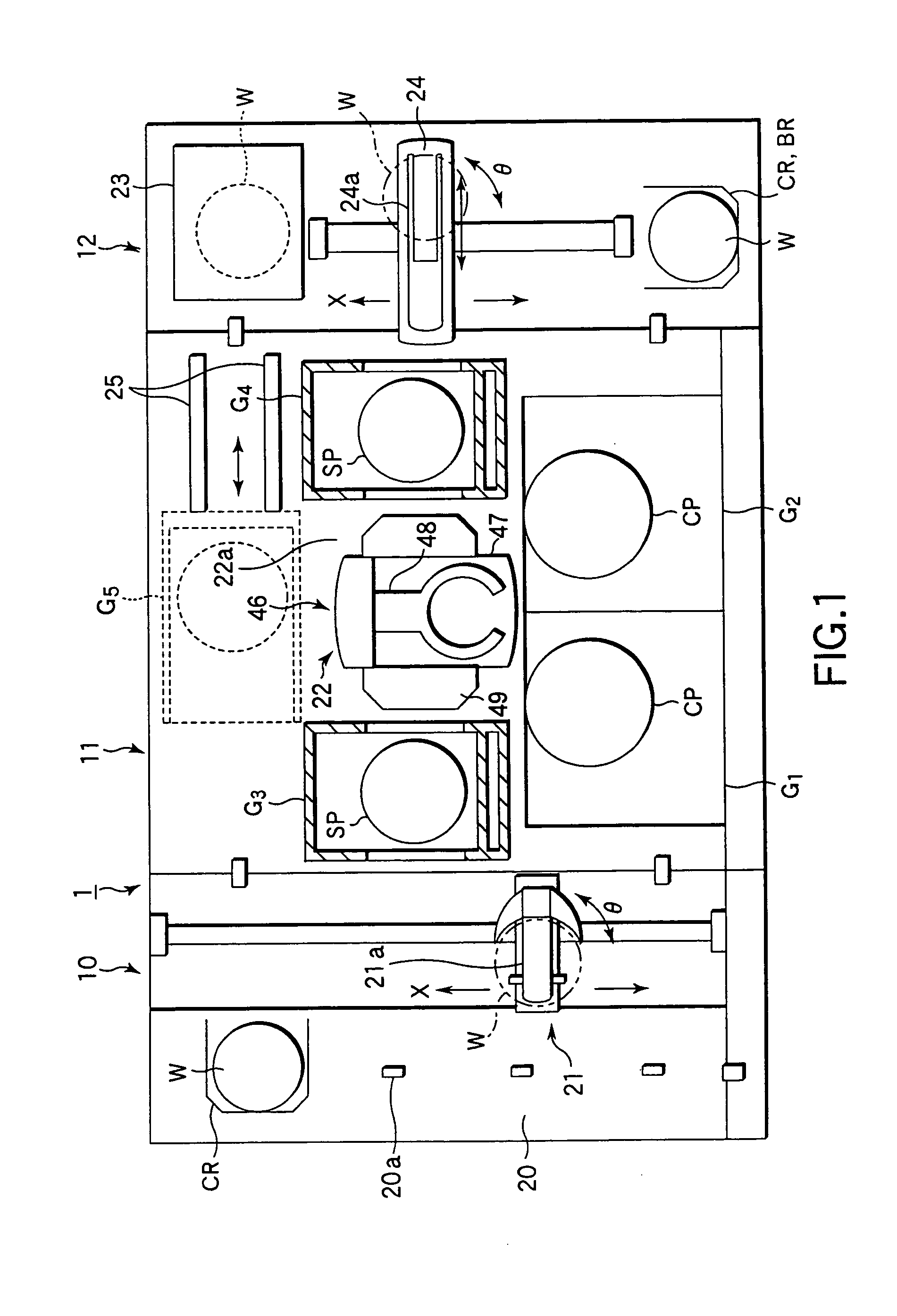
[0081] Some embodiments of the present invention will now be described in detail with reference to the accompanying drawings. Described in this case is a method for a developing processing using a resist coating and development system, which permits continuously carrying out the process steps ranging between the resist coating on a semiconductor wafer and the developing processing.

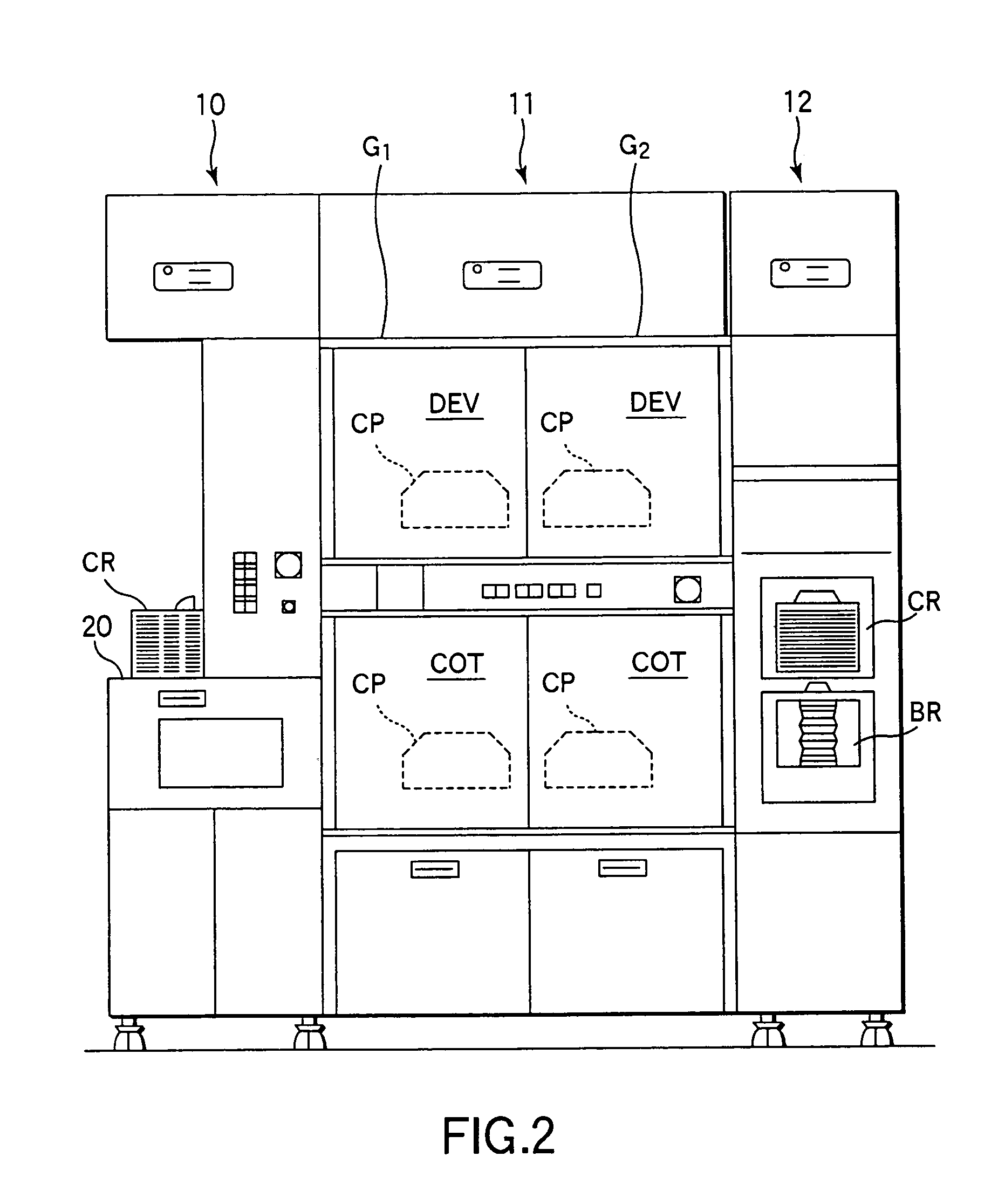
[0082]FIG. 1 is a plan view schematically showing the construction of a resist coating and development system 1. Further, FIGS. 2 and 3 are a front view and a back view, respectively, showing the construction of the resist coating and development system 1 shown in FIG. 1. As shown in the drawing, the resist coating and development system 1 comprises a cassette station 10 acting as a transfer station, a process station 11 provided with a plurality of process units, and an interface section 12 arranged adjacent to the process station 11 for the delivery of a wafer W between the process station 11 and an exp...


PUM


Abstract

In a developing processing of a wafer having a resist film low in the dissolving rate in a developing solution formed thereon and subjected to an exposure treatment, a developing solution of a low concentration is supplied first onto a wafer and the wafer is left to stand for a prescribed time to permit a developing reaction to proceed, followed by further supplying a developing solution having a concentration higher than that of the developing solution supplied first onto the wafer, leaving the substrate to stand and subsequently rinsing the wafer, thereby improving the uniformity of the line width in the central portion and the peripheral portion of the wafer.

Description

BACKGROUND OF THE INVENTION [0001] 1. Field of the Invention [0002] The present invention relates to a method for a developing processing of a substrate such as a semiconductor wafer subjected to an exposure treatment and an apparatus for supplying a developing solution. [0003] 2. Description of the Related Art [0004] In a manufacturing process of a semiconductor device, a prescribed circuit pattern is formed on the surface of a semiconductor wafer by using a so-called “photolithography technology”. In the photolithography step, a series of treatments are carried out such that a resist film is formed on a cleaned semiconductor wafer by supplying a photoresist solution onto the semiconductor wafer, followed by exposing the resist film to light in a prescribed pattern and subsequently developing the pattern. [0005] In the developing step, an exposed semiconductor wafer is held first by a rotatable spin chuck. Then, a puddle of a developing solution is formed by supplying a developing ...

Claims


Application Information

Patent Timeline
IPC IPC(8): G03D3/06G03F7/30H01L21/00H01L21/027
CPCG03D3/06H01L21/6715G03F7/3021H01L21/027
Inventor YOSHIHARA, KOUSUKETANAKA, KEIICHIYAMAMOTO, TAROKYOUDA, HIDEHARUTAKEGUCHI, HIROFUMIOOKOUCHI, ATSUSHI
Owner TOKYO ELECTRON LTD
Why Eureka
Try Eureka