Magnetic sensor and manufacturing method therefor
a technology of magnetic sensors and manufacturing methods, applied in the field of magnetic sensors, can solve the problems of not being able to accurately unable to always be able to measure the intensity of external magnetic fields, and non-uniform sensitivity direction of gmr elements, so as to improve the output stability of magnetic sensors, secure the output stability of the magnetic sensor rendering the external magnetic field, and secure the effect of uniform magnetization of the free layer
- Summary
- Abstract
- Description
- Claims
- Application Information
AI Technical Summary
Benefits of technology
Problems solved by technology
Method used
Image
Examples
first embodiment
1. First Embodiment
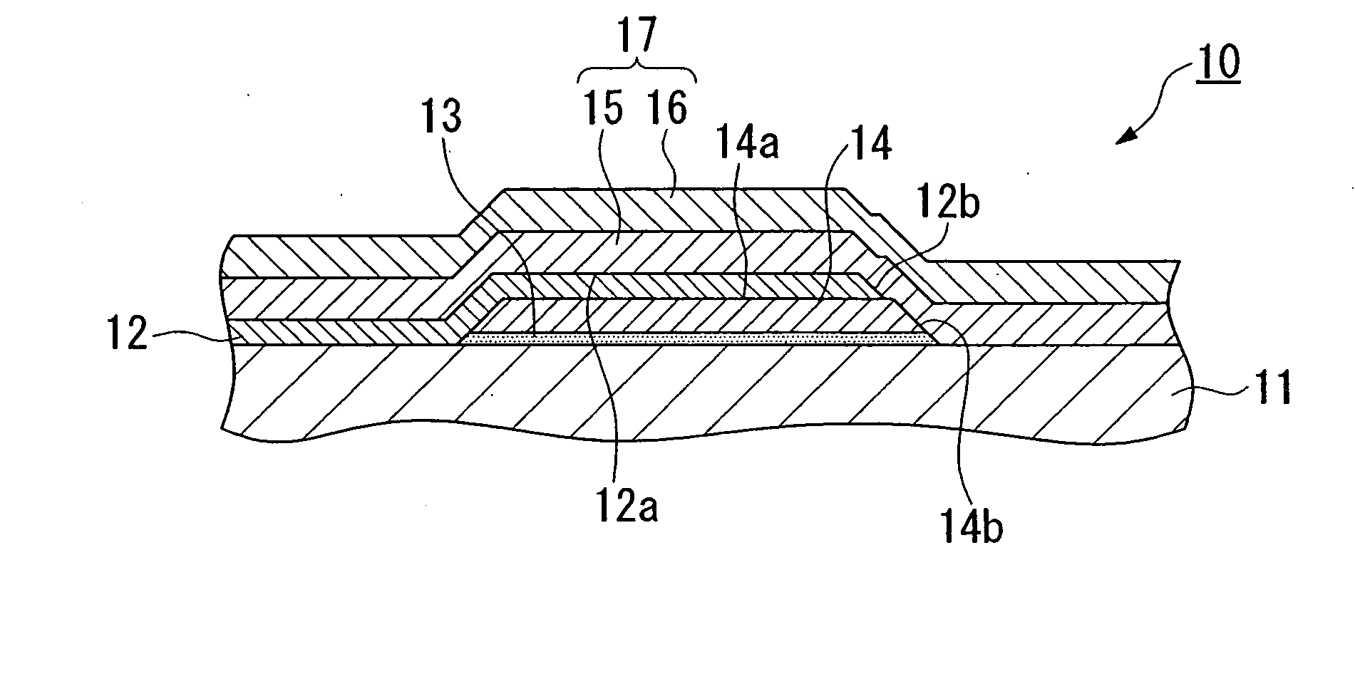
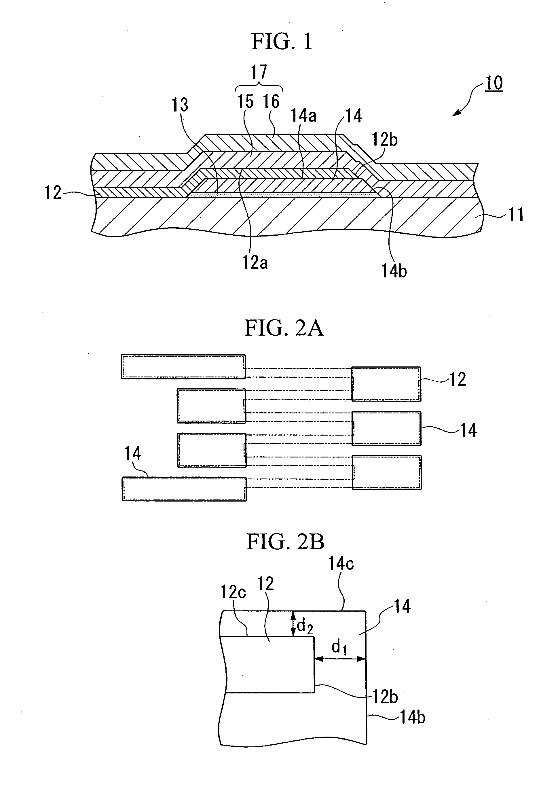
[0145]FIG. 1 is a cross-sectional view diagrammatically showing the constitution of a magnetic sensor in accordance with a first embodiment of the invention. FIGS. 2A and 2B provide illustrations showing a magnetoresistive element viewed from a protective film in the magnetic sensor shown in FIG. 1, wherein FIG. 2A is an overall illustration, and FIG. 2B is a fragmental illustration showing the peripheral portion of a bias magnet.
[0146] In FIG. 1, a magnetic sensor 10 comprises a substrate 11 composed of a quartz or silicon wafer having a prescribed thickness, a magnetoresistive element 12 composed of a GMR element arranged on the substrate 11, an embedded film 13 composed of a nonmagnetic material arranged on the substrate 11, a bias magnetic layer 14 composed of a permanent magnet film, which is connected to both ends of the magnetoresistive element 12 and is arranged on the substrate 11 via the embedded film 13, a first protective film 15 for covering the over...
second embodiment
2. Second Embodiment
[0197]FIG. 10 is a cross-sectional view diagrammatically showing the constitution of a magnetic sensor in accordance with a second embodiment of the invention.
[0198] A magnetic sensor 110 shown in FIG. 10 comprises a substrate 111 composed of a quartz or silicon wafer having a prescribed thickness, a magnetoresistive element 112 composed of a GMR element arranged on the substrate 111, an embedded film 113 composed of a nonmagnetic material arranged on the substrate 111, a bias magnetic layer 114 composed of a permanent magnet film, which is arranged on the substrate 111 via the embedded film 113 and which is connected with both ends of the magnetoresistive element 112 respectively, a first protective film 115 for entirely covering the magnetoresistive element 112 and the bias magnetic layer 114, a second protective film 116 for covering the upper surface of the first protective film 115, and an intermediate layer 118 that is arranged between the bias magnetic la...
third embodiment
3. Third Embodiment
[0216]FIG. 11 is a cross-sectional view diagrammatically showing the constitution of a magnetic sensor in accordance with a third embodiment of the invention.
[0217] A magnetic sensor 120 shown in FIG. 11 comprises a substrate 121 composed of a quartz or silicon wafer having a prescribed thickness, a magnetoresistive element 122 composed of a GMR element arranged on the substrate 121, an embedded film 123 composed of a nonmagnetic material arranged on the substrate 121, a bias magnetic layer 124 composed of a permanent magnet film, which is arranged on the substrate 121 via the embedded film 123 and which is connected with both ends of the magnetoresistive element 122 respectively, a first protective film 125 for entirely covering the magnetoresistive element 122 and the bias magnetic layer 124, a second protective film 126 for covering the upper surface of the first protective film 125, and an intermediate layer 128 that entirely covers an upper surface 124a of t...
PUM
 Abstract
Description
Claims
Application Information


