Acceleration sensor and manufacturing method thereof

Inactive Publication Date: 2005-03-17
LAPIS SEMICON CO LTD
View PDF2 Cites 27 Cited by
  • Summary
  • Abstract
  • Description
  • Claims
  • Application Information

AI Technical Summary

Benefits of technology

[0011] According to the present invention, since the acceleration sensor is formed in such a manner that the width of the support frame is narrower than the width of the pedestal all around its perimeter, the beams can be extended by a length corresponding to the reduced width of the support frame so that the parts of the beams will overlap the pedestal near their ends on the support frame side. Therefore, even when the acceleration sensor is made more compact, the deterioration of detection sensitivity can be prevented, thereby providing a compact, high-sensiti

Problems solved by technology

However, as the acceleration sensor becomes smaller in size, there arises a problem that the length of the beams becomes too short for the acceleration sensor to have sufficient sensitivity.
However, as the acceleration sensor is mi

Method used


Image

  • Acceleration sensor and manufacturing method thereof
  • Acceleration sensor and manufacturing method thereof
  • Acceleration sensor and manufacturing method thereof

Examples


Example

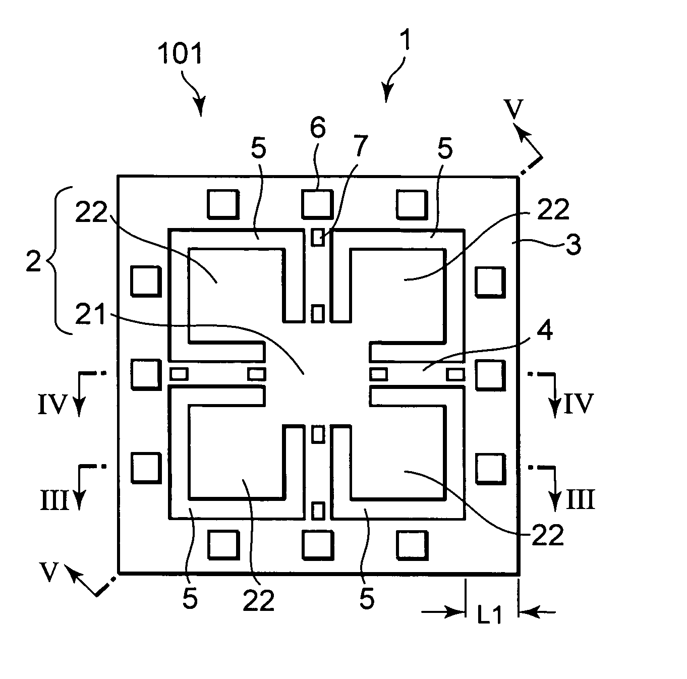
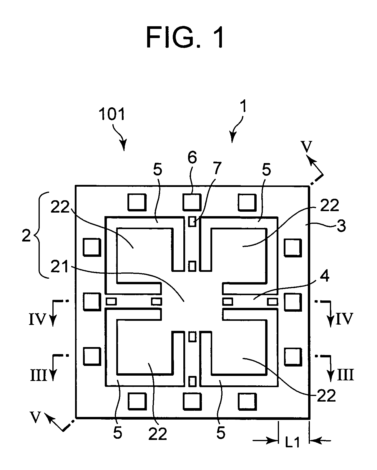
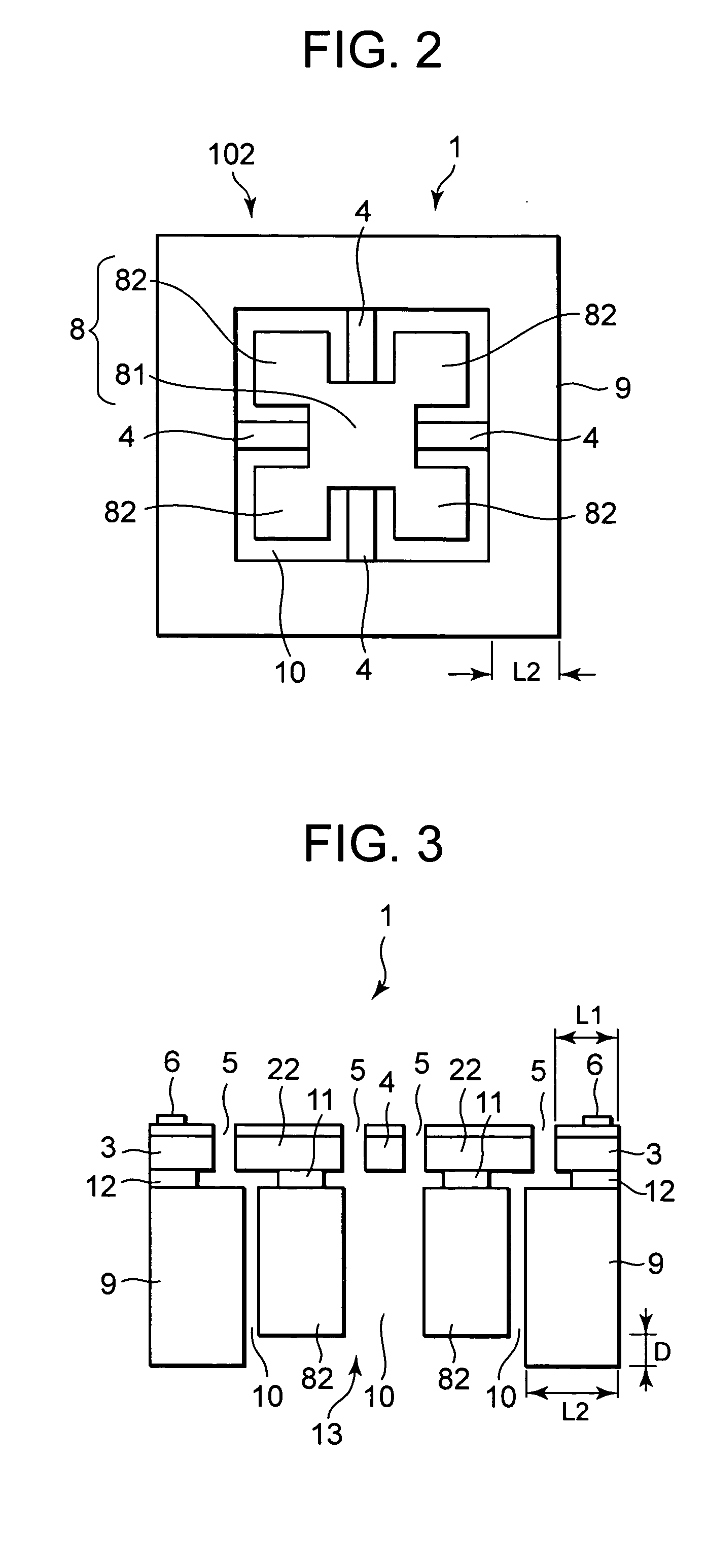
[0028] (1) Structure

[0029] An acceleration sensor according to the present invention will now be described by taking as an example a piezoresistive acceleration sensor 1 manufactured using an SOI (Silicon-On-Insulator) substrate as shown in FIG. 6. The SOI substrate is a semiconductor substrate with a first semiconductor film 101 and a second semiconductor film 102 formed on both sides of a dielectric film 103. In this case, the first semiconductor film 101 and the second semiconductor film 102 are made of Si, and the dielectric film 103 is SiO2. FIG. 1 is a plan view of the acceleration sensor 1 as viewed from the side of the first semiconductor film 101. FIG. 2 is a bottom view of the acceleration sensor 1 as viewed from the side of the second semiconductor film 102. FIG. 3 is a sectional view taken along the line III-III of FIG. 1, FIG. 4 is a sectional view taken along the line IV-IV of FIG. 1, and FIG. 5 is a sectional view taken along the line V-V of FIG. 1.

[0030] As shown i...


PUM

PropertyMeasurementUnit
Weightaaaaaaaaaa
Thicknessaaaaaaaaaa
Widthaaaaaaaaaa

Abstract

There is provided a compact, high-sensitivity acceleration sensor. The acceleration sensor includes a weight 8, a pedestal 9 arranged around the periphery of the weight 8, a support frame 3 formed to have a width narrower than the width of the pedestal 9 all around its perimeter, a mass 2 attached to the weight 8 to retain the weight 8 inside the support frame 3, beams 4 connecting the support frame 3 and the mass 2 and overlapping the pedestal 9 near their ends on the side of the support frame 3, and a peripheral interlayer 12 arranged between the support frame 3 and the pedestal 9 to create a predetermined clearance between the pedestal 9 and the parts of the beams 4 that overlap the pedestal 9.

Description

BACKGROUND OF THE INVENTION [0001] 1. Field of the Invention [0002] The present invention relates to an acceleration sensor that detects a change in resistance, capacitance, or voltage caused by the displacement of a mass supported by beams to determine acceleration, and a manufacturing method of the same. [0003] 2. Description of the Related Art [0004] Acceleration sensors are divided by sensing method into three types: piezoresistive, capacitive, and piezoelectric. For such types of acceleration sensors, there is known a structure in which a mass is supported by beams so that a change in resistance, capacitance, or voltage caused by the displacement of the mass will be detected to determine acceleration. In this structure, the longer the beams, the higher the sensitivity of the sensor. However, as the acceleration sensor becomes smaller in size, there arises a problem that the length of the beams becomes too short for the acceleration sensor to have sufficient sensitivity. [0005] ...

Claims


Application Information

Patent Timeline
IPC IPC(8): B81C1/00G01P15/08G01P15/09G01P15/12G01P15/125H01L29/84
CPCG01P15/0802G01P15/0922G01P15/18G01P15/125G01P15/123G01P2015/084G01P2015/0842
Inventor OZAWA, NOBUOKOBAYASHI, TAKASUMI
Owner LAPIS SEMICON CO LTD
Why Eureka
Try Eureka