

Parallel wiring and integrated circuit
a technology of parallel wiring and integrated circuits, applied in the direction of insulated conductors, flat/ribbon cables, cables, etc., can solve the problems of circuit area and power consumption, circuit components cannot be neglected, and it is difficult in principle to design a long-distance wiring line as an rc lumped constant circuit, and achieve excellent crosstalk robustness
- Summary
- Abstract
- Description
- Claims
- Application Information
AI Technical Summary
Benefits of technology
Problems solved by technology
Method used
Image

Examples
first embodiment
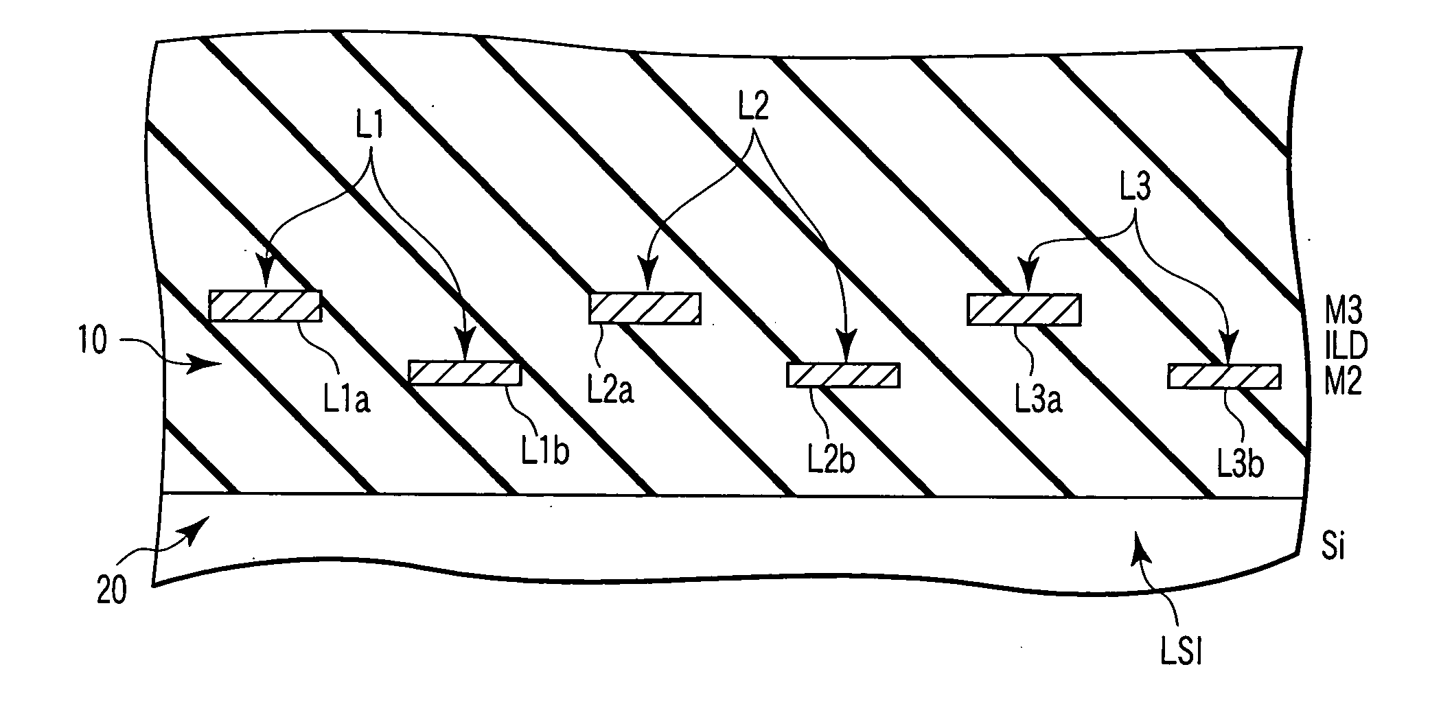
FIG. 1 is a longitudinal sectional view showing the wiring structure of a parallel wiring using differential transmission lines according to the FIG. 1 shows diagonal-pair lines.
Differential transmission lines L1, L2, and L3 shown in FIG. 1 are arranged in the horizontal direction above an Si (silicon) substrate 20 in an LSI. The differential transmission lines L1, L2, and L3 include pairs of substantially parallel signal wiring lines L1a and L1b, L2a and L2b, and L3a and L3b, respectively. The signal wiring lines of each differential transmission line have a diagonal structure in which they oppose each other obliquely with respect to the horizontal direction (reference direction). An ILD (interlayer dielectric film) 10 is formed between the wiring lines of each differential transmission line.
The signal wiring lines L1a, L1b, L2a, L2b, L3a, and L3b are made of a metal such as aluminum. The ILD 10 is made of SiO2 or the like. The layer including the signal wiring lines L1a, L2a, ...
second embodiment
FIGS. 12A and 12B are longitudinal sectional views showing parallel wiring structures using differential transmission lines according to the FIG. 12A shows stacked-pair lines. FIG. 12B shows co-planar lines.
Differential transmission lines L1 and L3 shown in FIG. 12A are arranged in the horizontal direction above an Si substrate 20 in an LSI. Differential transmission lines L2 and L4 are arranged in the horizontal direction at positions lower than the differential transmission lines L1 and L3 by two layers. The differential transmission lines L1 and L3 and differential transmission lines L2 and L4 are staggered in the horizontal direction.
The differential transmission lines L1, L2, L3, and L4 include pairs of substantially parallel signal wiring lines L1a and L1b, L2a and L2b, L3a and L3b, and L4a and L4b, respectively. The signal wiring lines of each differential transmission line are arranged in the vertical direction (reference direction). The signal wiring line L2a of the dif...
fourth embodiment
FIG. 14 is a longitudinal sectional view showing a parallel wiring structure using differential transmission lines according to the
Differential transmission lines L1, L2, L3, and L4 shown in FIG. 14 are arranged in the horizontal direction above an Si substrate 20 in an LSI. The differential transmission lines L1, L2, L3, and L4 include pairs of substantially parallel signal wiring lines L1a and L1b, L2a and L2b, L3a and L3b, and L4a and L4b, respectively. Referring to FIG. 14, for example, the signal wiring lines L1b and L3a are arranged between the signal wiring lines L2a and L2b. The signal wiring lines L2b and L4a are arranged between the signal wiring lines L3a and L3b.
Referring to FIG. 14, for example, the signal wiring line L3a of the differential transmission line L3 is arranged at the position where a coupling coefficient K between the signal wiring line L3a and the adjacent differential transmission line L2 is smaller than 0.1.
As described above, according to the firs...
PUM
 Abstract
Description
Claims
Application Information