CMOS transistors and methods of forming same

a technology of mos transistor and mos, which is applied in the direction of transistors, semiconductor devices, electrical equipment, etc., can solve the problems of increasing the source-drain resistance, and reducing so as to improve the performance of mos transistors and improve the device structure , improve the effect of operation

Inactive Publication Date: 2005-03-17
TEXAS INSTR INC
View PDF24 Cites 22 Cited by
  • Summary
  • Abstract
  • Description
  • Claims
  • Application Information

AI Technical Summary

Benefits of technology

[0009] The instant invention provides methods and systems for forming CMOS transistors that incorporate process steps for simultaneously improving the operation of both the P— and N-channel MOS devices. Further provided are the resulting improved device structures. More particularly there are provided herein solutions to obtaining more abrupt lateral profiles in ultra-shallow extension regions for improved CMOS transistor performance. As a result, the implant dose and / or energy at PLDD can be reasonably high to maintain a relatively low source-drain extension sheet resistance Rsd, while keeping gate-to-drain overlap capacitance and off-state leakage current in control.

Problems solved by technology

This often leads to an increase in the source-drain resistance of the MOS transistor, and results in degradation of the MOS transistor performance.
No single process has yet been provided which, to the inventor's knowledge, optimizes the performance of the P— and N-channel devices in a CMOS chip without diminishing the performance of the other.

Method used


Image

  • CMOS transistors and methods of forming same
  • CMOS transistors and methods of forming same
  • CMOS transistors and methods of forming same

Examples


Embodiment Construction

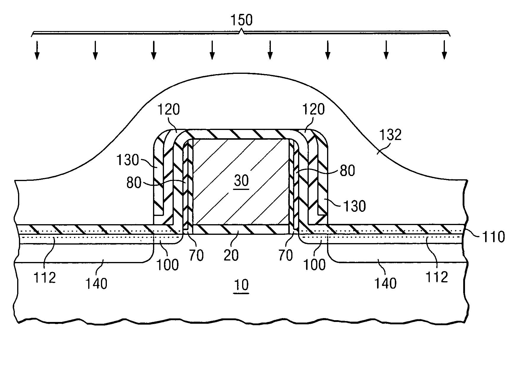
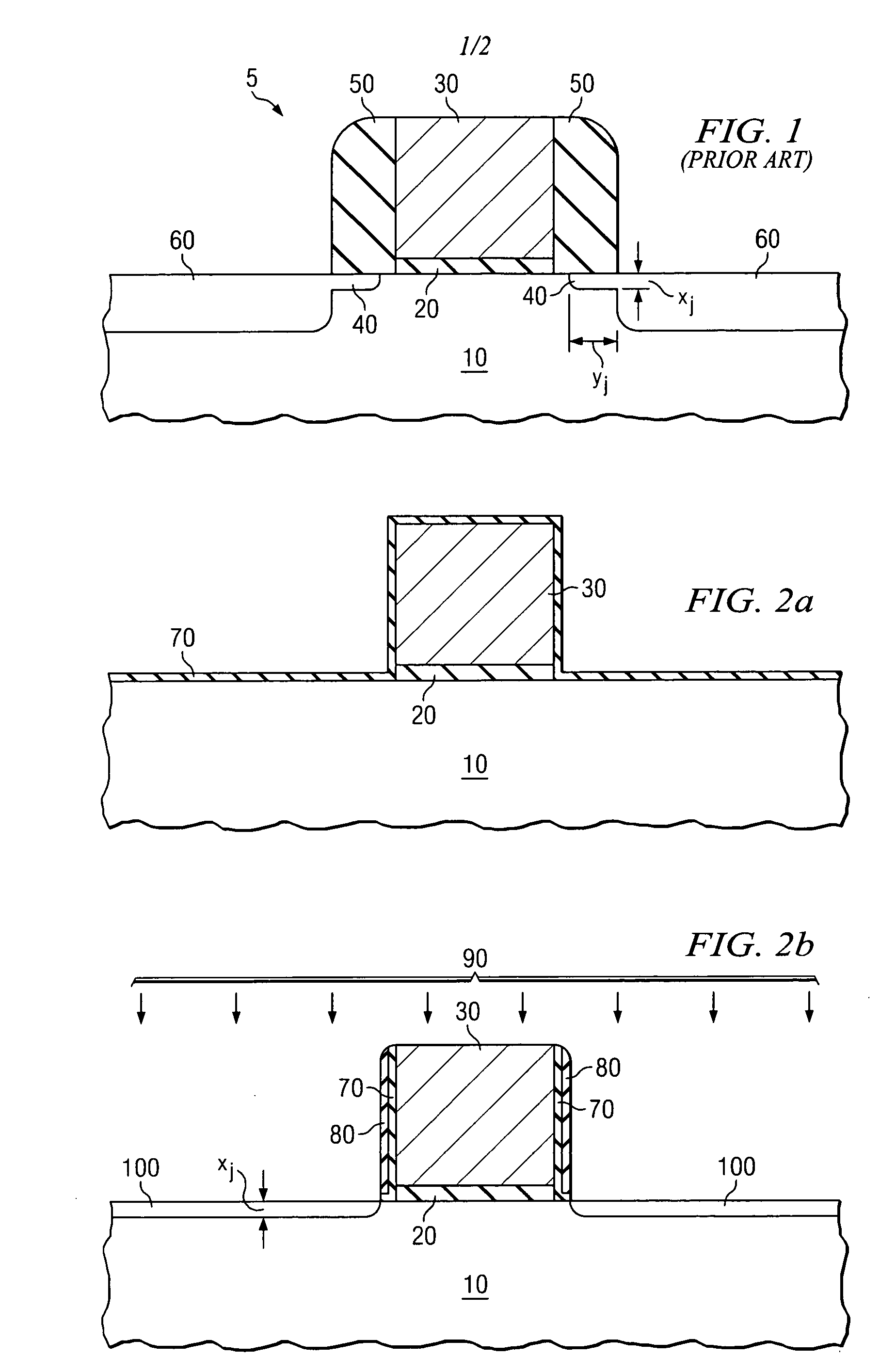
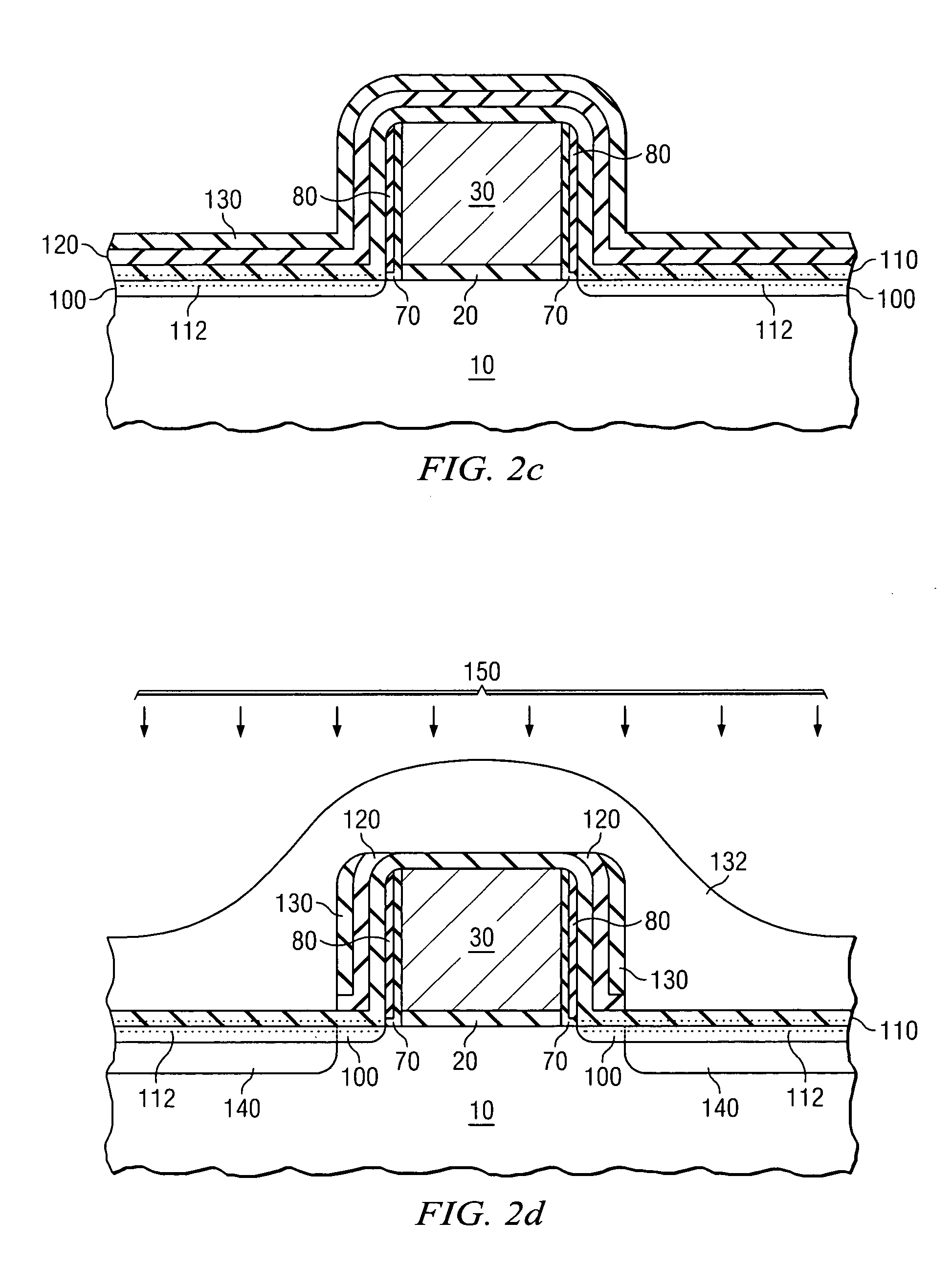
[0015] With reference to FIG. 2(a) the MOS transistors of the instant invention are fabricated on a semiconductor substrate 10. In one embodiment of the invention the substrate 10 is a silicon substrate with or without an epitaxial layer. The MOS transistors of the instant invention can also be formed on a silicon-on-insulator substrate that contains a buried insulator layer. Each MOS transistor is fabricated within an n-type or a p-type dopant region, or well, that is formed in the substrate 10. For purposes of illustrating the present invention, substrate 10 comprises an n-type well for the formation of a PMOS, or P-channel MOS transistor. It will be understood that an NMOS, or N-channel MOS transistor is formed in the identical manner within an adjacent p-type well (not shown).

[0016] In forming the MOS transistors of the instant invention, a gate dielectric region 20 is formed on the substrate 10. The gate dielectric region 20 can be formed using silicon oxide, silicon oxynitrid...


PUM


Abstract

The present invention teaches the formation of CMOS transistors using interfacial nitrogen at the interface between the lightly doped extension regions and an overlying insulating layer in combination with a capping layer of silicon nitride, both prior to the final source/drain anneal. Doses and energies may be increased for the P-channel lightly-doped drain, source and drain regions. The resulting transistors exhibit desirably high drive current and low off-state leakage current and overlap capacitance.

Description

CROSS-REFERENCE TO RELATED PATENT APPLICATIONS [0001] This application is a continuation-in-part of U.S. patent application Ser. No. 10 / 662,850, filed Sep. 15, 2003, titled: Integration of Pre-S / D Anneal Selective Nitride / Oxide Composite Cap for Improving Transistor Performance, by Bu, H. et al, the entirety of which is incorporated herein by reference.FIELD OF THE INVENTION [0002] The present invention relates generally to complementary metal oxide semiconductor (MOS) transistors and more particularly to methods for forming CMOS transistors having improved operating characteristics. BACKGROUND OF THE INVENTION [0003] Shown in FIG. 1 is a cross-sectional diagram of a typical metal oxide semiconductor (MOS) transistor 5. The MOS transistor 5 is fabricated in a semiconductor substrate 10. The MOS transistor comprises a gate dielectric layer 20 that is formed on the surface of the substrate 10. Typically this gate dielectric layer is formed using silicon oxide or nitrided silicon oxide...

Claims


Application Information

Patent Timeline
Patent Type & Authority Applications(United States)
IPC IPC(8): H01L21/00H01L21/265H01L21/3205H01L21/324H01L21/336H01L21/44H01L21/4763H01L21/8238H01L21/84H01L29/08H01L29/76H01L29/78
CPCH01L21/265H01L21/26506H01L21/26513H01L21/3185H01L21/324H01L21/823814H01L29/7845H01L29/0847H01L29/665H01L29/6656H01L29/6659H01L29/7833H01L29/7843H01L21/823864H01L21/2658H01L21/02255H01L21/02247H01L21/02216H01L21/02271H01L21/02211H01L21/02164H01L21/022
Inventor BU, HAOWENHORNUNG, BRIANCHIDAMBARAM, P.R.JAIN, AMITABHKHAMANKAR, RAJESHMAHALINGAM, NANDUCHAKRAVARTHI, SRINIVANSAN
Owner TEXAS INSTR INC
Why Eureka
Try Eureka