

Clock generating circuit
a clock generation and clock technology, applied in the direction of generating/distributing signals, pulse automatic control, pulse technique, etc., can solve the problems of large fluctuation of the generated clock b>6/b>, enhancing filter precision performance, and difficult integration of low-pass filters
- Summary
- Abstract
- Description
- Claims
- Application Information
AI Technical Summary
Benefits of technology
Problems solved by technology
Method used
Image

Examples
embodiment 1
[0033]
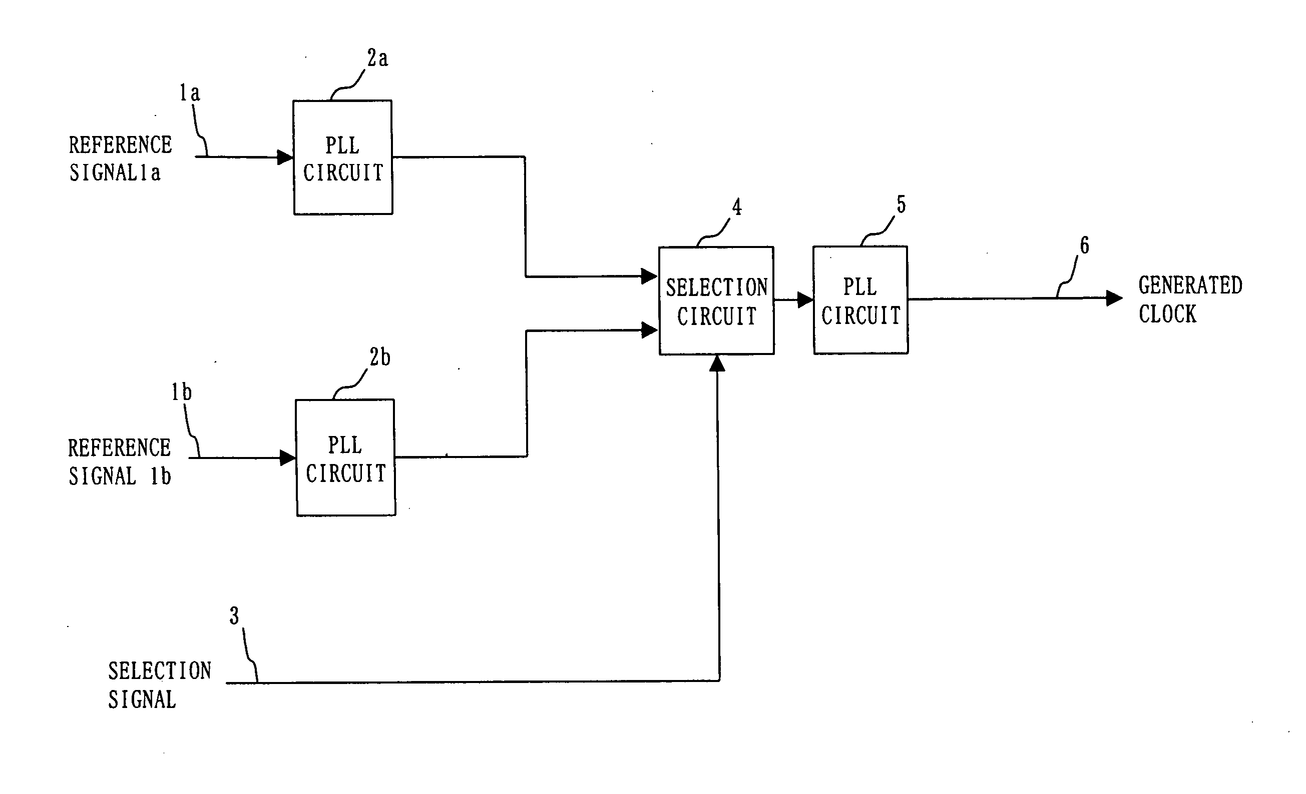
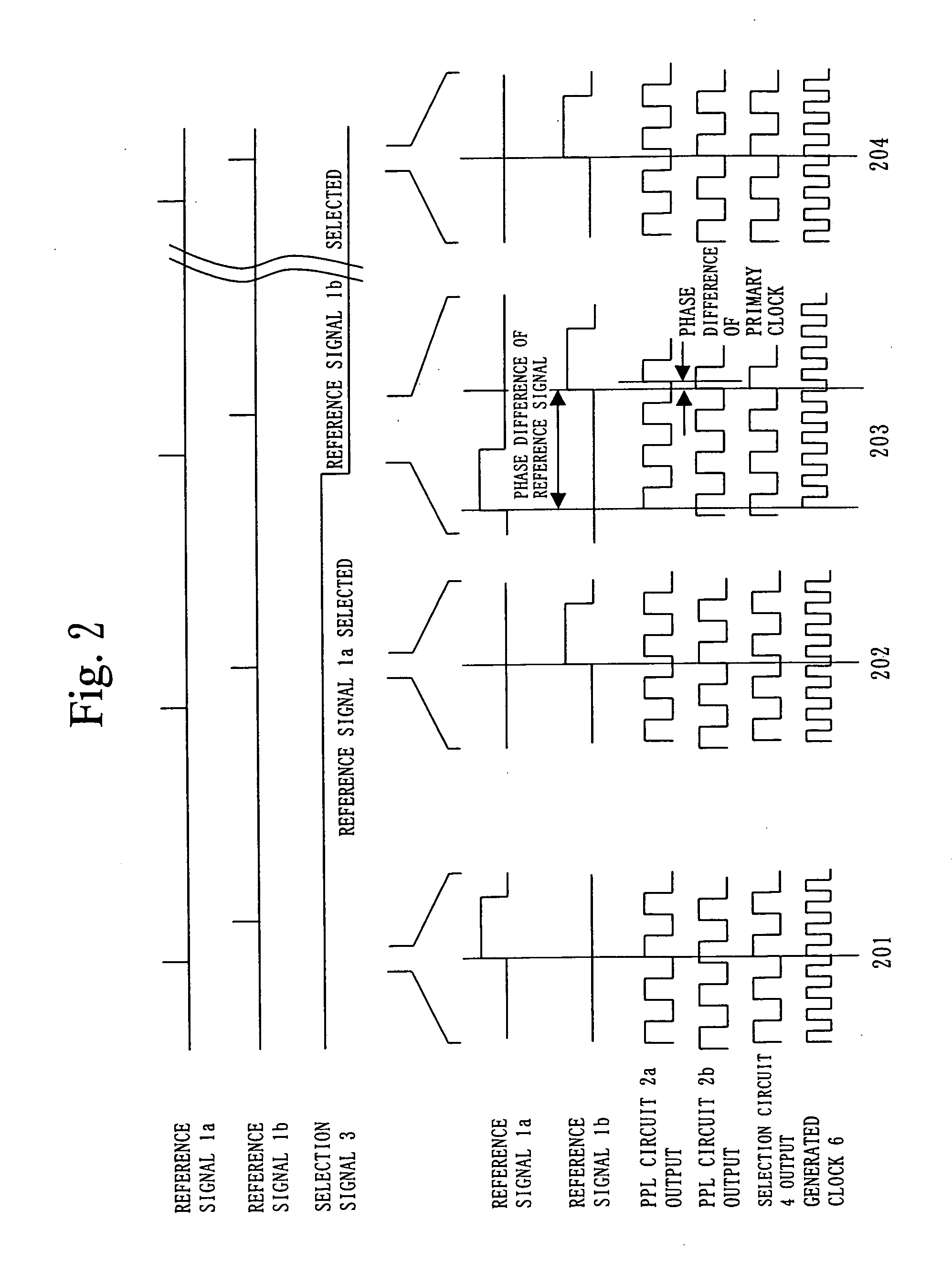
[0034] Hereinafter, a first embodiment is discussed with reference to FIG. 1. With referring to FIG. 1, a reference numeral 1 denotes a reference signal, a reference numeral 2 denotes a PLL circuit, a reference numeral 3 denotes a selection signal, a reference numeral 4 denotes a selection circuit, a reference numeral 5 denotes a PLL circuit, and a reference numeral 6 denotes a generated clock. FIG. 2 shows the waveform of each element in FIG. 1.
[0035] As shown in FIG. 1, the reference signals 1 are inputted, respectively, to the PLL circuits 2. More specifically, a reference signal 1a is inputted to a PLL circuit 2a, and a reference signal 1b is inputted to a PLL circuit 2b. The PLL circuits 2a and 2b output primary clocks that are synchronized, respectively, with the reference signals 1a and 1b inputted.
[0036] Then, the selection circuit 4 selects one of the primary clocks that are synchronized with the reference signals outputted from the PLL circuits 2, respectively, bas...
embodiment 2
[0044]
[0045] A second embodiment is now discussed with reference to the drawings. With referring to FIG. 3, a reference numeral 1 denotes a reference signal, a reference numeral 2 denotes a PLL circuit (former stage), a reference numeral 3 denotes a selection signal, a reference numeral 4 denotes a selection circuit, a reference numeral 5 denotes a PLL circuit (latter stage), a reference numeral 6 denotes a generated clock, a reference numeral 7 denotes a phase control circuit, a reference numeral 8 denotes a phase comparator circuit, and a reference numeral 9 denotes a control circuit.
[0046] According to the second embodiment, the phase control circuits 7 are provided, respectively, at the outputs of the PLL circuits 2 receiving the reference signals 1, so that the phase of the primary clock outputted from the phase control circuit 7 through the PLL circuit 2 corresponding to the reference signal 1 selected in the selection circuit 4 based on the selection signal 3 and the phase o...
embodiment 3
[0048]
[0049] According to a third embodiment, the phase control circuit 7 discussed in the second embodiment is implemented by a ring counter and a selection circuit.
[0050] With referring to FIG. 4, a reference numeral 1 denotes a reference signal, a reference numeral 2 denotes a PLL circuit (former stage), a reference numeral 7 denotes a phase control circuit, a reference numeral 10 denotes flip-flops, a reference numeral 11 denotes a NOR circuit, a reference numeral 12 denotes a selection circuit, a reference numeral 13 denotes a control signal, and a reference numeral 14 denotes an output of the phase control circuit. FIG. 5 shows the waveform of each element in FIG. 4.
[0051] The primary clock outputted from the PLL circuit 2 operates a ring counter that is configured with flip-flops 10 and the NOR circuit 11. As shown in FIG. 5, outputs from a flip-flop 10a˜a flip-flop 10y are multi-phase signals depending upon the number of the stages in the ring counter. Selecting one of the...
PUM
 Abstract
Description
Claims
Application Information