Film pattern formation method, device and method for manufacturing the same, electro-optical device, electronic device, and method for manufacturing active matrix substrate

Active Publication Date: 2005-03-24
ELEMENT CAPITAL COMMERCIAL CO PTE LTD
View PDF3 Cites 51 Cited by
  • Summary
  • Abstract
  • Description
  • Claims
  • Application Information

AI Technical Summary

Benefits of technology

[0011] In the film pattern formation method according to the present invention, the functional liquid is disposed in the area partitioned by banks, and a film pattern is formed on the substrate after the functional liquid is dried, for example. In this case, since the shape of film patterns are defined by the banks, further progress in the fineness of a film pattern and the further miniaturization thereof can be attained by forming the banks appropriately, for example, by reducing the width of a groove defined by the banks.
[0032] According to the present invention as described above, since fine film patterns can be formed with high precision in a stable manner, accordingly, it is possible to manufacture an active matrix substrate which can provide the desired performance.

Problems solved by technology

The photolithography method requires large equipment, such as vacuum equipment, and complex processing steps.
In addition, the manufacturing cost of the photolithography method is high since the efficiency of material usage is as low as several percent, and most of the material needs to be disposed of.
In the film pattern formation method using the liquid drop ejection method described above, since ejected liquid drops spread on the substrate after they land on the substrate, it has been difficult to form fine film patterns in a stable manner.

Method used


Image

  • Film pattern formation method, device and method for manufacturing the same, electro-optical device, electronic device, and method for manufacturing active matrix substrate
  • Film pattern formation method, device and method for manufacturing the same, electro-optical device, electronic device, and method for manufacturing active matrix substrate
  • Film pattern formation method, device and method for manufacturing the same, electro-optical device, electronic device, and method for manufacturing active matrix substrate

Examples


second embodiment

[0133] In the following, a second embodiment of the present invention will be explained with reference to the drawings.

[0134]FIG. 6 is a diagram schematically illustrating a film pattern formation method according to the present invention.

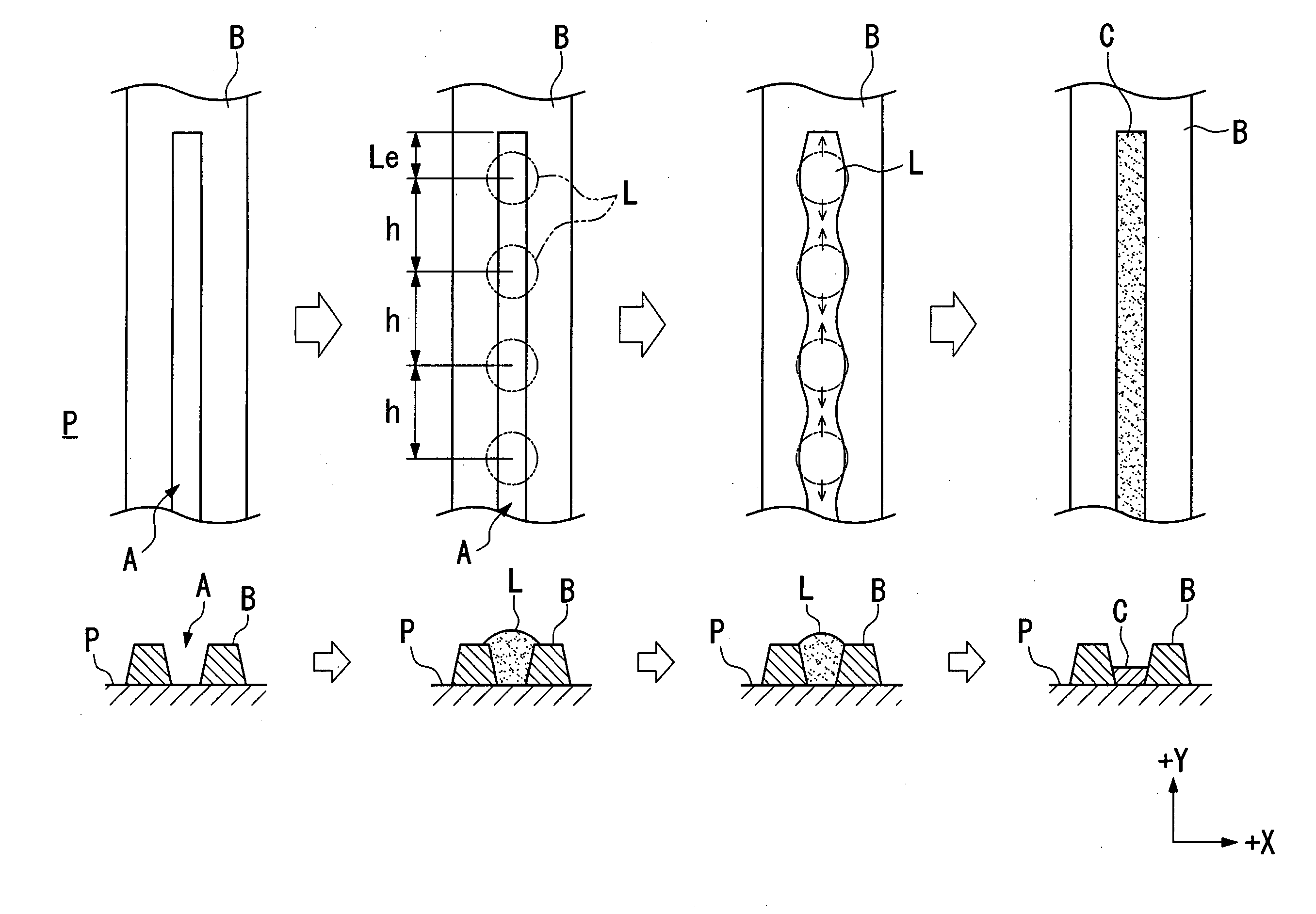
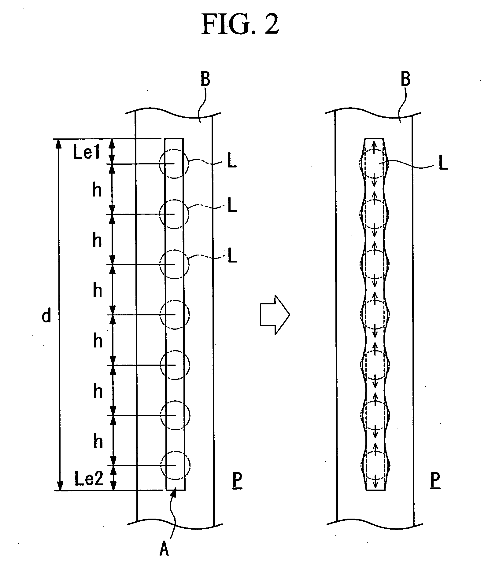
[0135] The film pattern formation method according to the present invention includes a liquid repelling layer forming step for forming a liquid repelling layer F in a desired pattern having repellency to functional liquid on a substrate P, and a material disposing step for disposing functional liquid L to a linear area A partitioned by the liquid repelling layer F.

[0136] As methods for forming the liquid repelling layer F, it is possible to use, for example, a method for forming a self assembled layer on a substrate, plasma processing (plasma polymerization), eutectoid plating, and a method for imparting liquid repellency with gold thiol. For example, a liquid repelling layer F in a desired pattern can be formed on a substrate by imparting liqui...

third embodiment

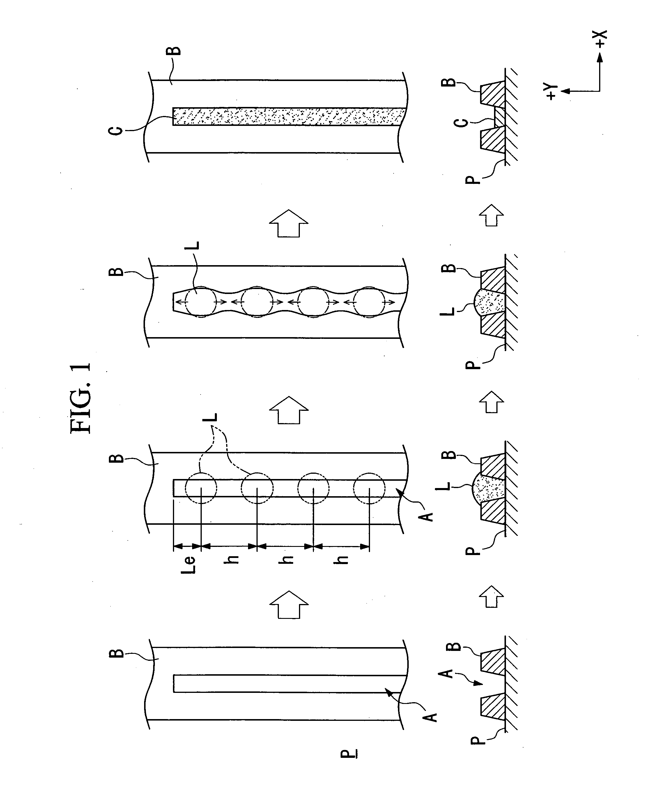
[0160] Next, with reference to FIGS. 8A-E, a method of forming conductive film wiring on a substrate will be explained as an example of embodiments of the method of forming a wiring pattern according to the present invention.

[0161] The film pattern formation method according to this embodiments disposes the above-mentioned ink for wiring patterns (wiring pattern formation material) on a substrate to form an electrically conductive film pattern for the wiring on the substrate, and generally includes a surface treatment step (liquid repelling layer forming step), a material disposing step and intermediate drying step, and a thermal treatment / photo treatment step.

[0162] Hereinafter, each step will be explained in detail.

[0163] (Surface Treatment Step)

[0164] The surface treatment step is classified broadly into the liquid-repelling treatment step which imparts liquid-repellency to a substrate surface, and the liquid-affinity treatment step which imparts to affinity with liquid to th...


PUM

PropertyMeasurementUnit
Electrical conductivityaaaaaaaaaa
Areaaaaaaaaaaa

Abstract

A method for forming a film pattern on a substrate includes the steps of: forming banks on the substrate; and making liquid drops of functional liquid land on the substrate to dispose the liquid drops in an area partitioned by the banks, wherein a spacing between the liquid drops are determined so that the liquid drops connect together after they land on the substrate, and a position in which a liquid drop of the liquid drops which lands the closest to an end of the area is spaced from the end of the area by less than a half of the spacing between the liquid drops.

Description

BACKGROUND OF THE INVENTION [0001] 1. Field of the Invention [0002] The present invention relates to a film pattern formation method, a device and method for manufacturing the same, an electro-optical device, an electronic device, and a method for manufacturing an active matrix substrate. [0003] Priority is claimed on Japanese Patent Application Nos. 2003-151288 and 2003-151289 filed May 28, 2003, and Japanese Patent Application No. 2004-095975, filed Mar. 29, 2004, the contents of which are incorporated herein by reference. [0004] 2. Description of Related Art [0005] As a method for forming film patterns, e.g., wiring patterns, used in electronic circuits or integrated circuits, a photolithography method is used, for example. The photolithography method requires large equipment, such as vacuum equipment, and complex processing steps. In addition, the manufacturing cost of the photolithography method is high since the efficiency of material usage is as low as several percent, and mo...

Claims


Application Information

Patent Timeline
IPC IPC(8): B05D1/26B05D5/12B05D7/00G02F1/1368B41J2/14C23C4/12C23C26/02G02F1/1345G09F9/00H01L21/28H01L21/288H01L21/3205H01L21/336H01L21/768H01L29/786H01L51/00H01L51/40H01L51/50H05B33/10H05K3/12
CPCB41J2/14201B41J2202/09C23C4/121C23C26/02H05K2203/1173H01L21/76838H01L51/0005H05K3/125H05K2201/09909H01L21/288C23C4/123H10K71/135A01G31/02Y02P60/21
Inventor MIKOSHIBA, TOSHIAKI
Owner ELEMENT CAPITAL COMMERCIAL CO PTE LTD
Why Eureka
Try Eureka