Semiconductor radiation detector and radiological imaging apparatus

Inactive Publication Date: 2005-03-31
HITACHI LTD
View PDF10 Cites 24 Cited by
  • Summary
  • Abstract
  • Description
  • Claims
  • Application Information

AI Technical Summary

Benefits of technology

[0006] A feature of a first embodiment of the invention for solving the above described problem is a semiconductor radiation detector comprising a plurality of semiconductor detection devices, each having an anode electrode on one side of a semiconductor device and a cathode elect

Problems solved by technology

However, the device described in JP-A-2003-84068 can detect γ-rays mainly on a plane of incidence of γ-rays (e.g., X-Y plane) by separating their positions but cannot detect γ-rays in the direction of incidence of

Method used


Image

  • Semiconductor radiation detector and radiological imaging apparatus
  • Semiconductor radiation detector and radiological imaging apparatus
  • Semiconductor radiation detector and radiological imaging apparatus

Examples


first embodiment

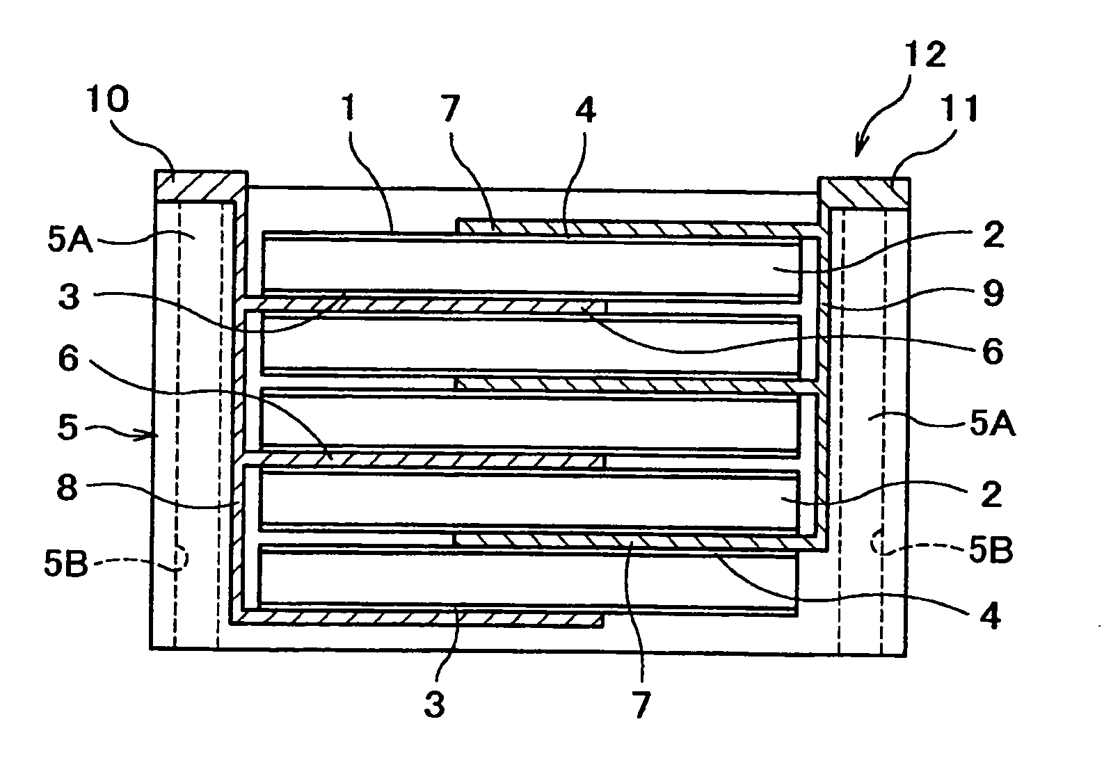
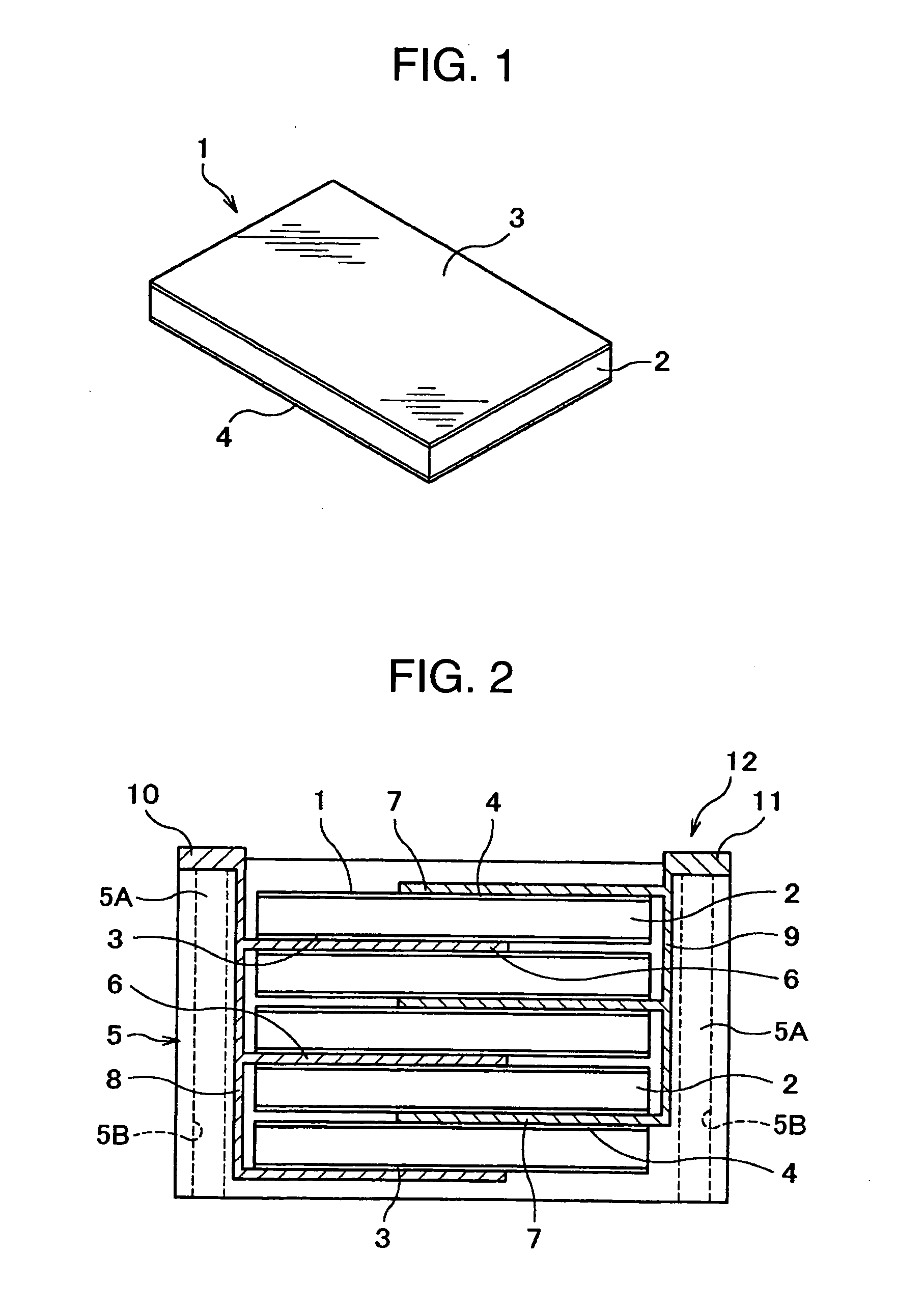
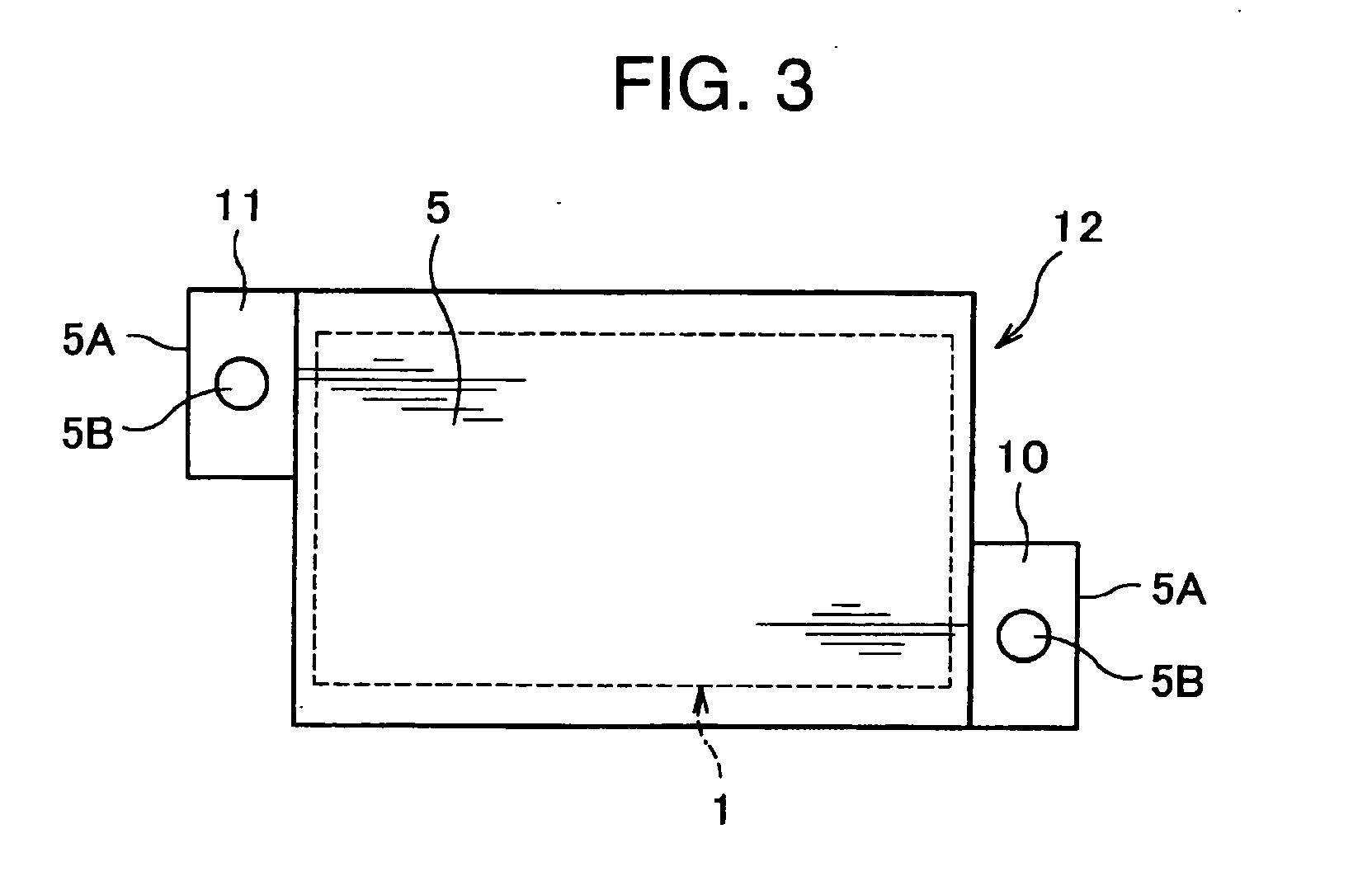
[0034] Reference numeral 1 in FIG. 1 denotes a radiation detection device and this radiation detection device 1 is constructed by including five semiconductor devices 2 (see FIG. 2) made up of a rectangular flat plate made of, for example, CdTe, cathode electrodes 3 (Pt, etc.) formed into a thin-film shape on one side of each semiconductor device 2 by means of, for example, vapor deposition, anode electrodes 4 (In, etc.) formed into a thin-film shape on the other side of the semiconductor device 2 and a rectangular parallelepiped elastic insulator 5 (see FIG. 2) which covers the five semiconductor devices 2 from the outside.

[0035] As shown in FIG. 2, this semiconductor radiation device 1 consists of five semiconductor devices 2 stacked together. Furthermore, conductive cathode-side thin plates 6 are pasted to the respective cathode electrodes 3 and conductive anode-side thin plates 7 are pasted to the respective anode electrodes 4. First and second internal wirings 8, 9 provide con...

second embodiment

[0045] Then, a second embodiment of the present invention will be explained with reference to the attached drawings of FIG. 6 and FIG. 7. In FIG. 6, a plurality of semiconductor radiation detectors 31 are constructed by including thin wiring boards 32 with flexibility called “FPC (Flexible printed circuit)”, semiconductor devices 33 mounted on both sides of the thin wiring boards 32, cathode electrodes 34 formed in a thin-film shape on one side of the semiconductor devices 33 through vapor deposition, etc., and anode electrodes 35 formed on the other side of the semiconductor devices 33.

[0046] The semiconductor devices 33 are arranged in four rows in the direction in which γ-rays propagate with a small gap interposed between neighboring devices and also arranged in four rows in the direction orthogonal to the direction in which γ-rays propagate with a small gap interposed between neighboring devices. Furthermore, the semiconductor radiation detectors 31 are mounted fixed to both si...

third embodiment

[0052] Then, a third embodiment of the present invention will be explained with reference to the attached drawing of FIG. 8. The same components in this embodiment as those in the first embodiment are assigned the same reference numerals and explanations thereof will be omitted.

[0053] As shown in FIG. 8, a PET-X-ray CT examination apparatus 100, which is a radiation imaging apparatus, comprises an X-ray CT examination apparatus 101 and a PET examination apparatus 102 side by side. Furthermore, the PET-X-ray CT examination apparatus 100 includes a bed holding section 103 and a movable bed 104 provided on the bed holding section 103. Then, the X-ray CT examination apparatus 101 is provided with an X-ray CT gantry 105 having an opening 105A, a rotary section 106 rotatably mounted in the X-ray CT gantry 105, an X-ray generator 107 provided in the rotary section 106 and a radiation detector 108, which is a scintillator detector provided in the rotary section 106. Then, this X-ray CT exa...


PUM


Abstract

A radiation imaging apparatus with high spatial resolution including semiconductor radiation detectors arranged on a wiring board capable of detecting γ-rays by separating their positions in the direction of incidence of γ-rays is provided. A semiconductor radiation detector is constructed by including five semiconductor devices made up of, for example, CdTe rectangular parallelepiped plates, a cathode electrode on one side of the semiconductor device, an anode electrode on the other side of the semiconductor device and an insulator for coating five semiconductor detection devices from the outside. The semiconductor radiation detector is mounted on a wiring board using an anode pin and a cathode pin.

Description

BACKGROUND OF THE INVENTION [0001] The present invention relates to a semiconductor radiation detector, which allows semiconductor radiation detectors to be arranged in a three-dimensional direction and a radiation imaging apparatus using the same. [0002] A semiconductor radiation detector is provided with a semiconductor device made of CdTe, CdZnTe, etc., and electrodes formed on both sides of this semiconductor device designed to pick up electric charge generated when radiation such as X-rays or γ-rays enter the semiconductor device by applying a bias voltage between these electrodes from the electrodes as a signal. [0003] When a semiconductor radiation detector is used for a medical radiation imaging apparatus, etc., the semiconductor radiation detector is connected on a wiring board to form a radiation detection section (see JP-A-2003-84068 (paragraph 00024, FIG. 3), for example). [0004] A PET (Positron Emission Tomography), which is a kind of a medical radiation imaging apparat...

Claims


Application Information

Patent Timeline
IPC IPC(8): G01T1/24A61B6/03G01T1/161G01T1/29H01L27/14H01L31/09H04N5/30
CPCA61B6/037G01T1/2928
Inventor YANAGITA, NORIHITOKITAGUCHI, HIROSHIISHITSU, TAKAFUMIAMEMIYA, KENSUKEUENO, YUUICHIROUTSUCHIYA, KATSUTOSHIKOJIMA, SHINICHIYOKOI, KAZUMA
Owner HITACHI LTD
Why Eureka
Try Eureka