

Nuclear medicine imaging apparatus
a technology of nuclear medicine and imaging apparatus, applied in the direction of instruments, radiation measurement, measurement devices, etc., can solve the problems of increasing the time for imaging, poor energy resolution, deterioration of images, etc., and achieve the effect of improving the cooling efficiency of the semiconductor radiation detector and improving the accuracy of radiation detection
- Summary
- Abstract
- Description
- Claims
- Application Information
AI Technical Summary
Benefits of technology
Problems solved by technology
Method used
Image

Examples
embodiment 1
[0048] [Embodiment 1]
[0049] Nuclear Medicine Imaging Apparatus
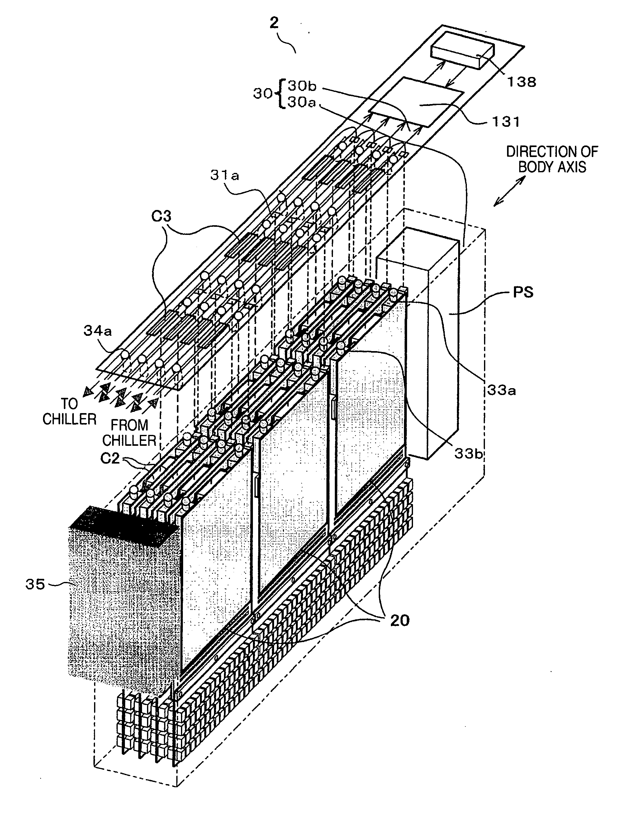
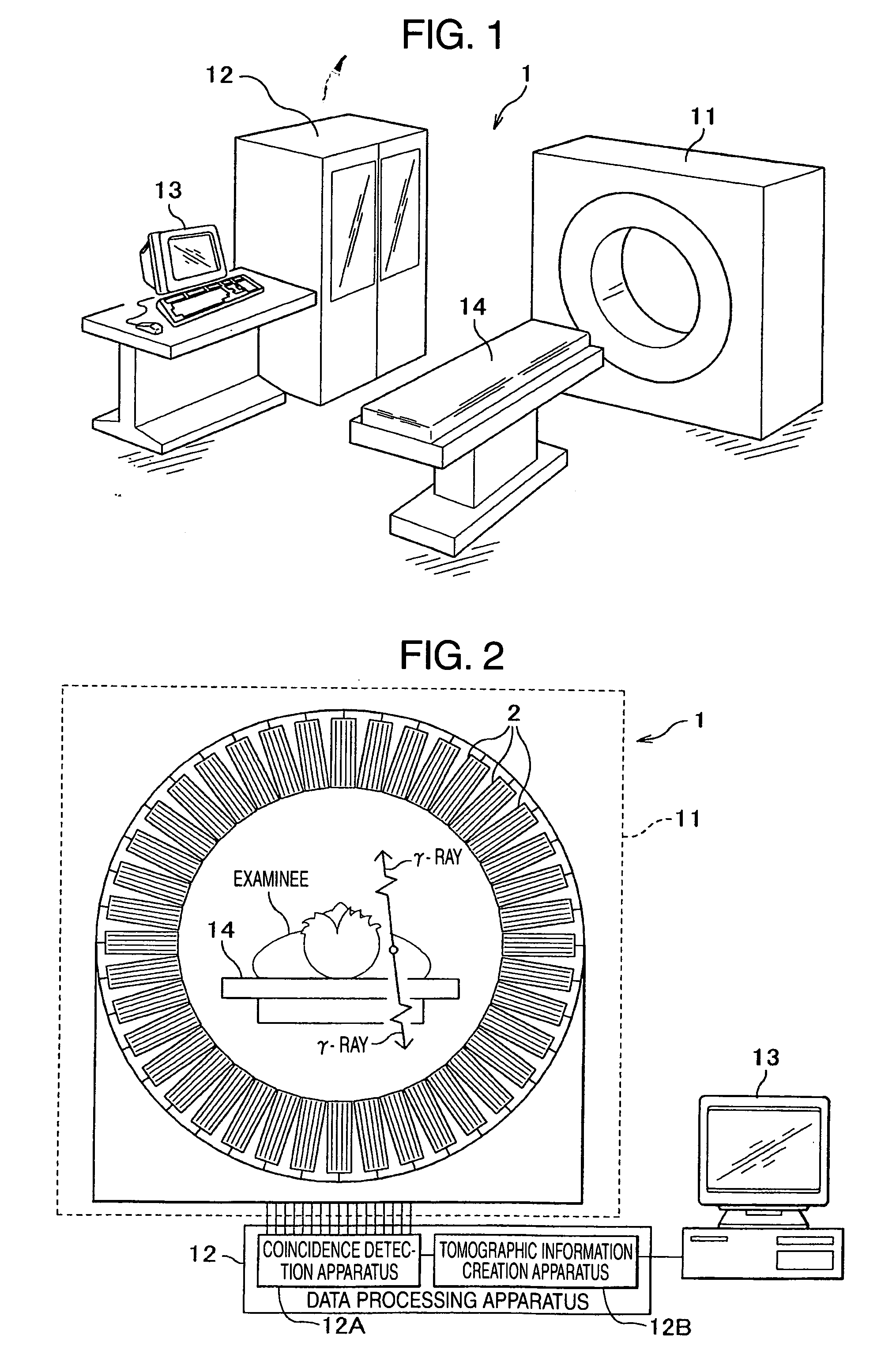
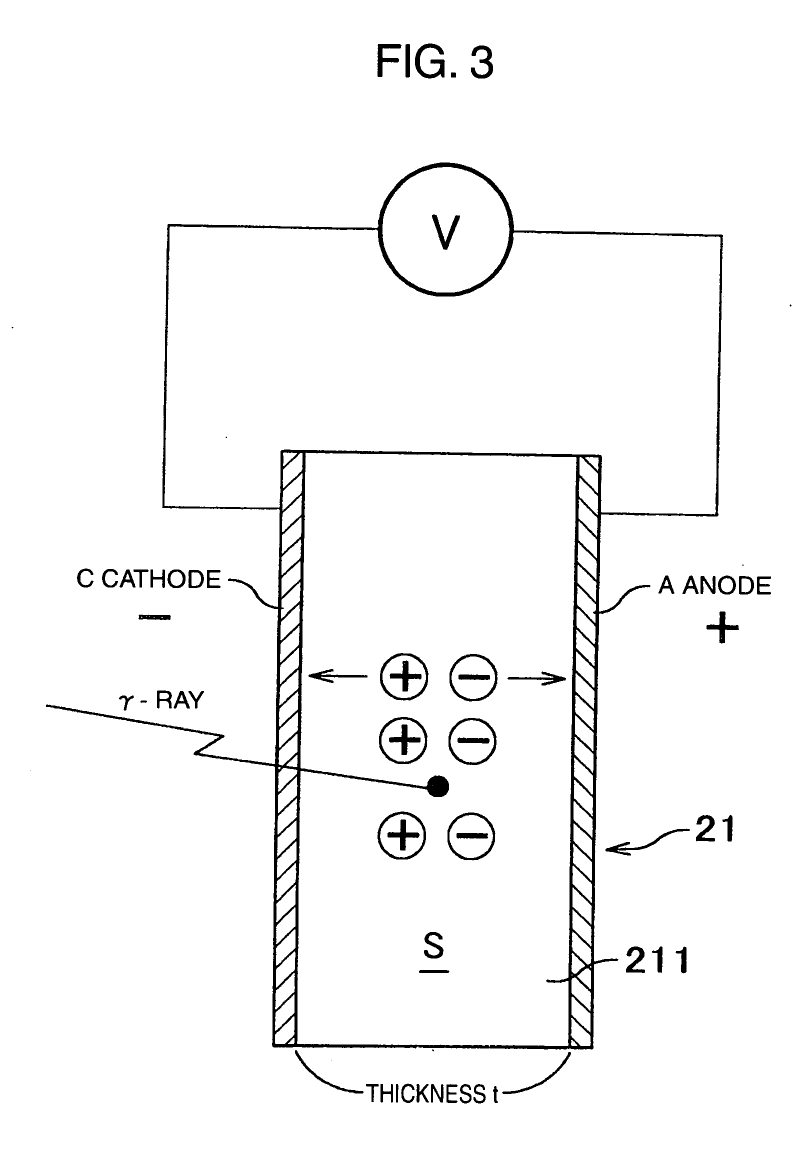
[0050] At first, the nuclear medicine imaging apparatus (radiological imaging apparatus) of Embodiment 1 will be described. As shown in FIG. 1, a PET apparatus 1 as a nuclear medicine imaging apparatus is configured to comprise a camera (imaging apparatus) 11, a data processing apparatus 12 and a display apparatus 13. An examinee (subject) is loaded on the bed 14 so as to be imaged by the camera 11. The camera 11 has a great number of built-in semiconductor radiation detectors 21 so as to detect gamma rays emitted out of the body of an examinee with the semiconductor radiation detectors 21 (hereinafter referred to simply as detector) 21. The camera 11 comprises an integrated circuit (ASIC) that the peak value i.e. energy and detection time of the detected radiation (γ-ray) are measured. The data processing apparatus 12 has a storage apparatus, a coincidence detection apparatus 12A (to be referred to in FIG. 2), and a tom...
embodiment 2
[0139] [Embodiment 2]
[0140] Next, Embodiment 2 will be described with a SPECT apparatus as an example. This SPECT apparatus 51 will be described with reference to FIGS. 13 to 16 and FIG. 21. The SPECT apparatus 51 comprises, as shown in FIG. 13, a pair of radiation detectors 52, a rotating support stand 57, a data processing apparatus 12A and a display apparatus 13. Those radiation detectors 52 are disposed in a rotation support stand 57 in positions subject to displacement such as 180° and 90° in the circumferential direction. In addition, the radiation detectors 52 respectively rotates independently so as to enable incident angles to change and with 2 units being arranged side by side the imaging area can be extended, or otherwise the radiation detectors 52 can be used as a gamma camera to conduct plane imaging. A radiation detector 52 comprises 32 sets of ASICs boards 53B and one detector board 20C, detectors 21A and a collimator 55, configuring itself one camera unit. The ASIC b...
PUM
 Abstract
Description
Claims
Application Information