Process for fabricating thin film transistors

a thin film transistor and fabrication process technology, applied in transistors, semiconductor devices, electrical equipment, etc., can solve the problems of less satisfactory amorphous silicon semiconductor layer, substrate swelling, and temperature which can be employed

Inactive Publication Date: 2005-03-31
E INK CORPORATION
View PDF99 Cites 137 Cited by
  • Summary
  • Abstract
  • Description
  • Claims
  • Application Information

AI Technical Summary

Problems solved by technology

However, the polyimide used in the process described in the latter paper, sold commercially under the name “Kapton” (Registered Trade Mark) has a glass transition temperature of only about 300° C., which restricts the temperatures which can be employed during the fabrication process, and results in a less satisfactory amorphous silicon semiconductor layer.
This polyimide also has a high moisture absorption (about 4 percent by weight) and such high moisture absorption can result in swelling of the substrate and consequent cracking of thin layers deposited on the substrate, or delamination of thin layers from the substrate.

Method used


Image

  • Process for fabricating thin film transistors
  • Process for fabricating thin film transistors
  • Process for fabricating thin film transistors

Examples


Embodiment Construction

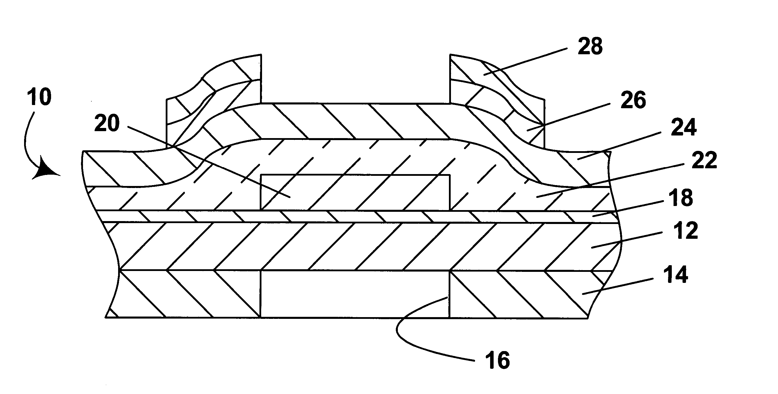
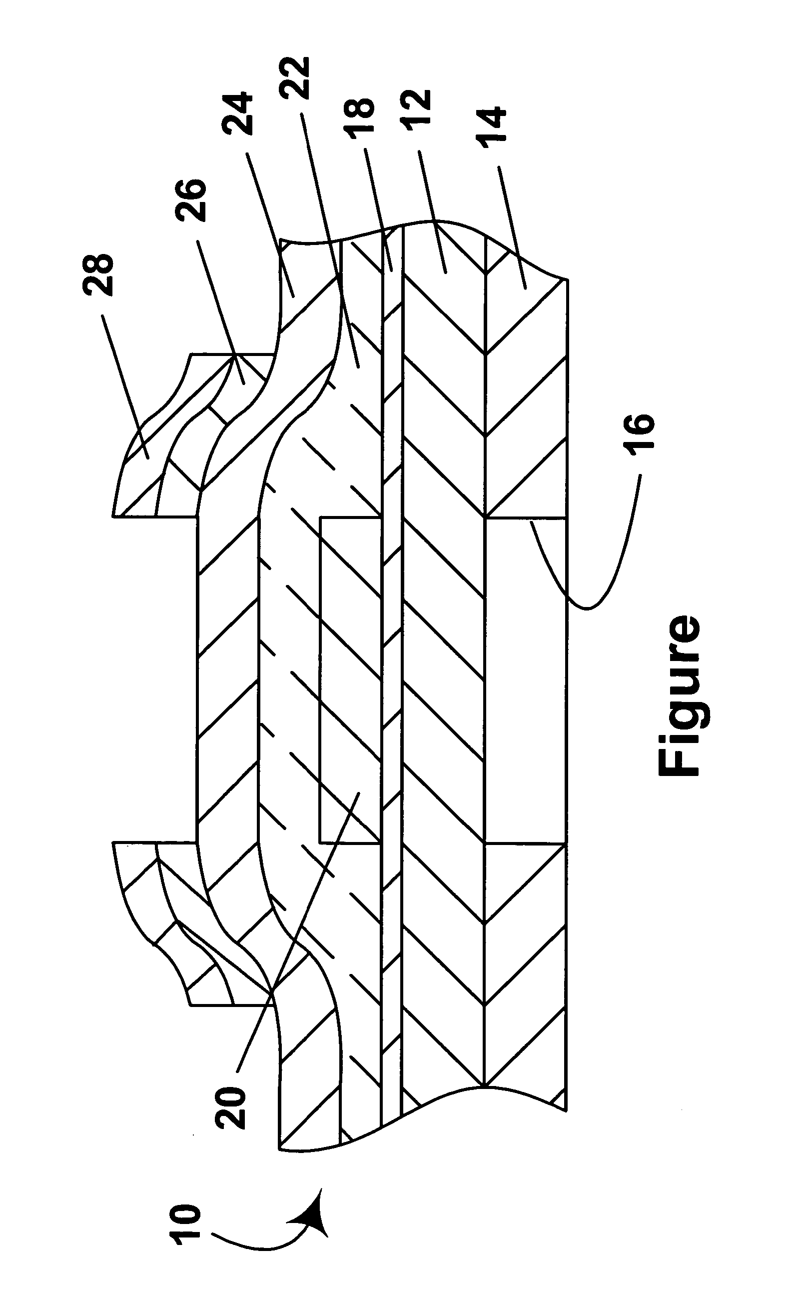
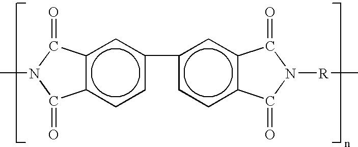
Preferred polyphenylene polyimides for use in the present process are those sold commercially under the trade names Upilex-S and Upilex-VT by UBE America, Inc., 55 East 59th Street, 18th Floor, New York N.Y. 10022. Both these materials are stated by the manufacturer to be of the formula:

in which R is an alkylene group. These polyimides are derivatives of biphenyl-3,3′,4,4′-tetracarboxylic acid and an α,ω-alkanediamine, for example 1,6-hexamethylene diamine (formally hexane-1,6-diamine). The main difference between the two materials is that Upilex-S is a simple polyimide film, while Upilex-VT is surface-treated on one face to facilitate hot lamination of the film, without adhesive, to ceramics or metal foils. For purposes of the present invention, the Upilex VT may be laminated to a stainless steel backing film. Another preferred polyimide for use in the present process is Upilex-50SS, from the same manufacturer.

Polyphenylene polyimides have glass transition temperatures consid...


PUM

PropertyMeasurementUnit
thicknessaaaaaaaaaa
glass transition temperatureaaaaaaaaaa
temperaturesaaaaaaaaaa

Abstract

Transistors are formed by depositing at least one layer of semiconductor material on a substrate comprising a polyphenylene polyimide. The substrate permits the use of processing temperatures in excess of 300° C. during the processes used to form the transistors, thus allowing the formation of high quality silicon semiconductor layers. The substrate also has a low coefficient of thermal expansion, which closely matches that of silicon, thus reducing any tendency for a silicon layer to crack or delaminate.

Description

BACKGROUND OF THE INVENTION This invention relates to a process for fabricating thin film transistors. Thin film transistors (TFT's) are known to be useful for, inter alia, controlling various types of display; for example TFT's are commonly used to control liquid crystal displays used in portable computers and similar electronic devices. TFT's can also be used to control electrophoretic displays; see, for example, Applications Ser. No. 60 / 132,642, filed May 5, 1999 and Ser. No. 09 / 565,413, filed May 5, 2000; Applications Ser. No. 60 / 144,943, filed Jul. 21, 1999, 60 / 147,989, filed Aug. 10, 1999, and Ser. No. 09 / 621,000, filed Jul. 22, 2000; Applications Ser. No. 60 / 151,547, filed Aug. 31, 1999, and Ser. No. 09 / 652,486, filed Aug. 31, 2000; Applications Ser. Nos. 60 / 151,715 and 60 / 151,716, both filed Aug. 31, 1999, and Ser. No. 09 / 651,710, filed Aug. 31, 2000; and Applications Ser. No. 60 / 151,549, filed Aug. 31, 1999 and Ser. No. 09 / 650,620, filed Aug. 30, 2000. The disclosures of ...

Claims


Application Information

Patent Timeline
Patent Type & Authority Applications(United States)
IPC IPC(8): H01L21/336H01L29/786
CPCH01L29/78603H01L29/66765H01L29/786
Inventor DENIS, KEVIN L.CHEN, YUDRZAIC, PAUL S.JACOBSON, JOSEPH M.KAZLAS, PETER T.
Owner E INK CORPORATION
Why Eureka
Try Eureka