Package having integral lens and wafer-scale fabrication method therefor

a technology of integral lenses and wafers, applied in the field of microstructure elements, can solve the problems of not teaching structures or methods, the formation of terminals on caps and vias for connecting terminals to contacts on active wafers requires a relatively complex series of steps, and the 511 patent is considerably larger than the unit itsel

Inactive Publication Date: 2005-03-31
TESSERA INC
View PDF98 Cites 88 Cited by
  • Summary
  • Abstract
  • Description
  • Claims
  • Application Information

AI Technical Summary

Problems solved by technology

This increases the area of active wafer required to form each unit, requires additional operations and results in an assembly considerably larger than the unit itself.
However, formation of terminals on the caps and vias for connecting the terminals to the contacts on the active wafer requires a relatively complex series of steps.
Moreover, the '511 patent does not teach structures or methods which permit lenses or other optically active elements to be incorporated into the caps.

Method used


Image

  • Package having integral lens and wafer-scale fabrication method therefor
  • Package having integral lens and wafer-scale fabrication method therefor
  • Package having integral lens and wafer-scale fabrication method therefor

Examples


Embodiment Construction

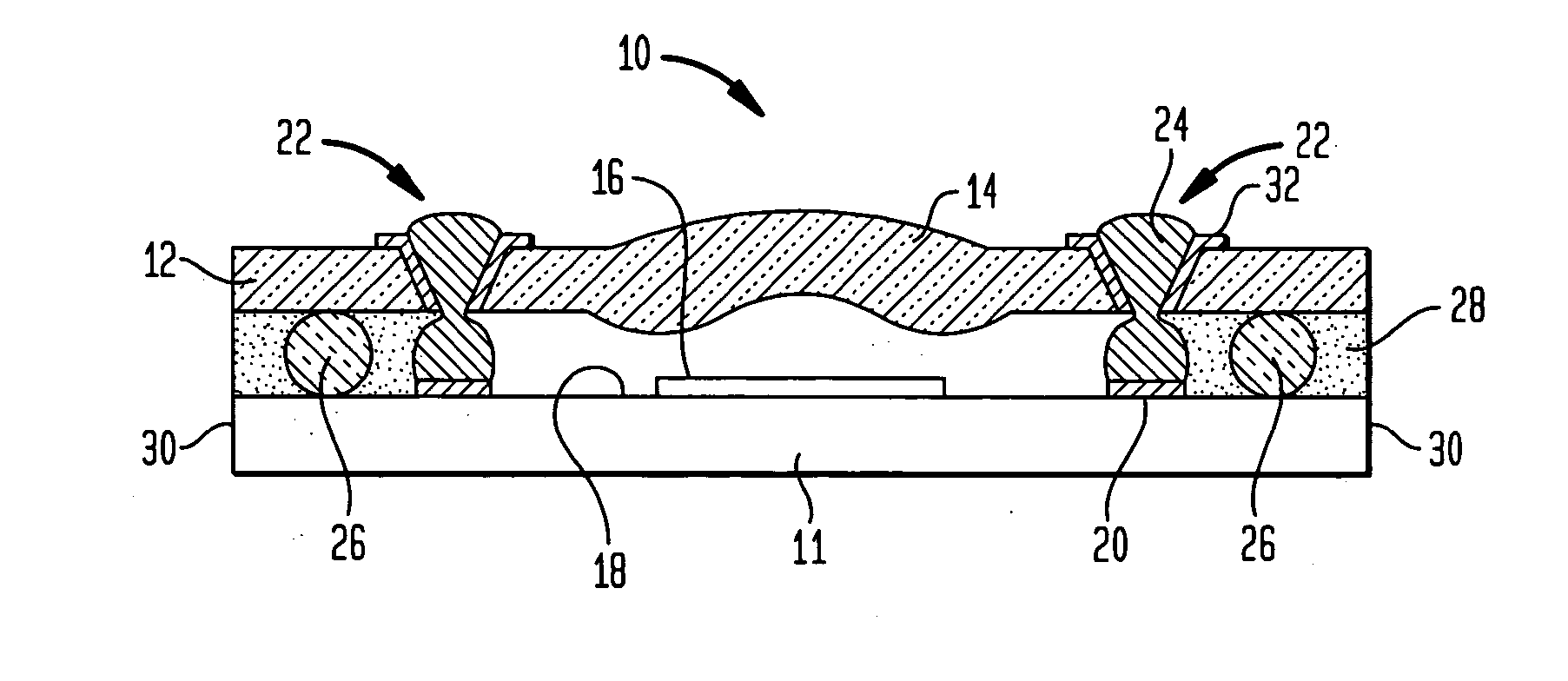
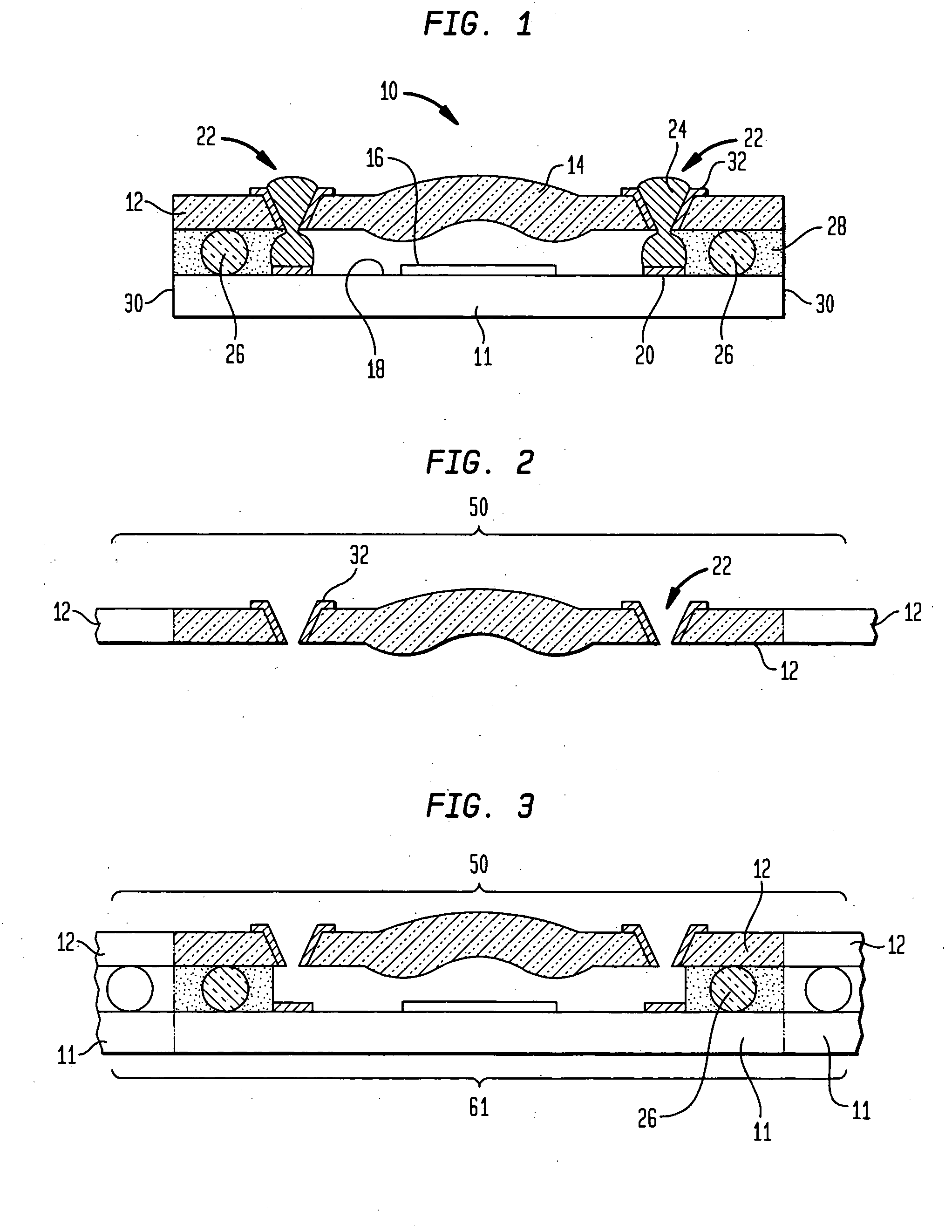
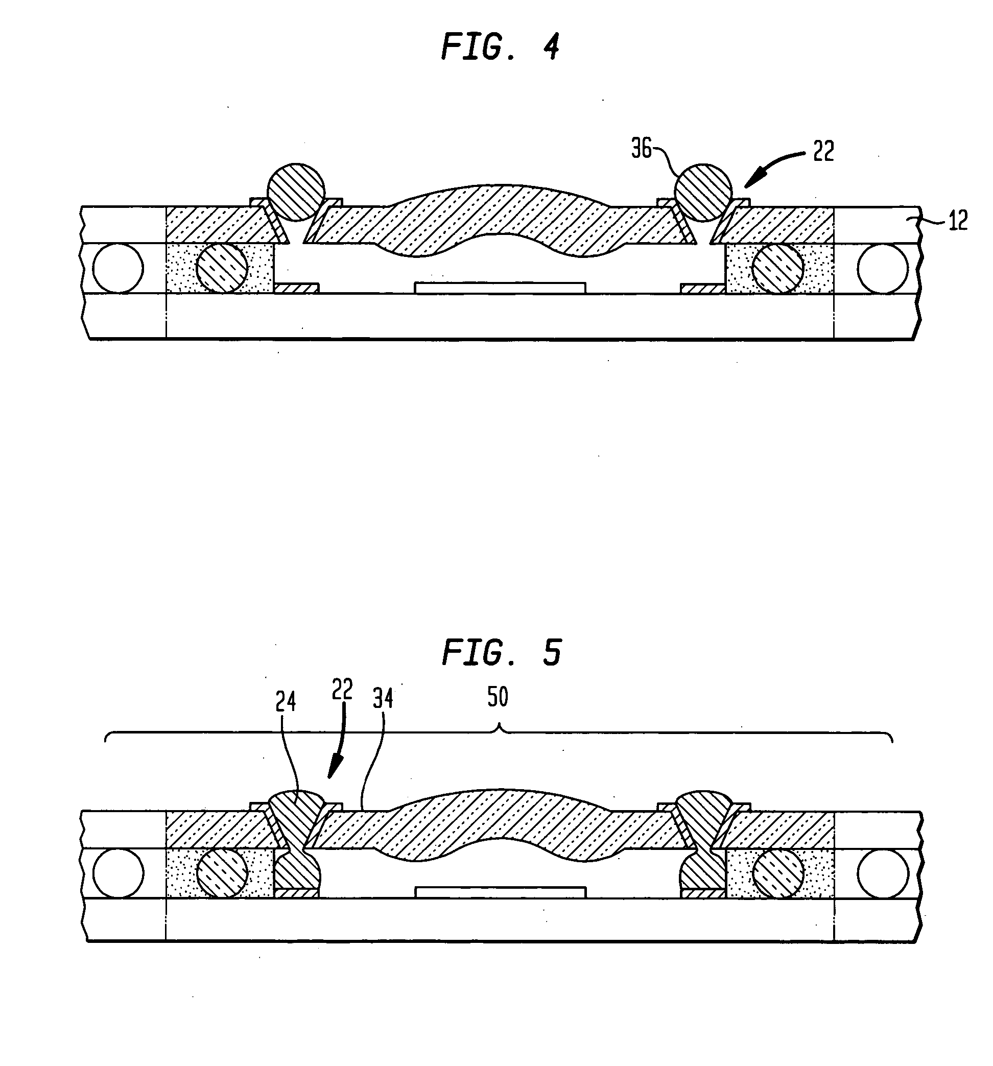
[0017] Microelectronic elements such as semiconductor chips or “dies” commonly are provided in packages which protect the die or other element from physical damage, and which facilitate mounting of the die on a circuit panel or other element.

[0018] One type of microelectronic package includes a cap, which encloses a cavity overlying an active area of the packaged chip. For example, commonly owned U.S. Provisional Application No. 60 / 449,673 filed Feb. 25, 2003 and commonly owned, co-pending U.S. patent application Ser. No. 10 / 786,825 filed Feb. 25, 2004, the disclosures of which are hereby incorporated by reference herein, describe ways of mounting caps to chips, especially at a wafer scale, to permit the making of interconnects to the front surfaces of the chips from outside an area in which an active device area of the chip is located.

[0019] The embodiments of the invention address a particular need to provide a method of packaging chips having optoelectronic devices such as imag...


PUM


Abstract

A covered chip having an optical element integrated in the cover is provided which includes a chip having a front surface, an optically active circuit area, and bond pads disposed at the front surface. The chip is covered by an at least partially optically translucent or transparent unitary cover that is mounted to the front surface of the chip, and has at least one optical element integrated in the unitary cover. The cover is further aligned with the optically active circuit area and vertically spaced from the optically active circuit area.

Description

CROSS-REFERENCE TO RELATED APPLICATIONS [0001] This application claims the benefit of U.S. Provisional Application No. 60 / 568,041 filed on May 4, 2004, entitled “Structure And Method Of Making Capped Chips”; U.S. Provisional Application No. 60 / 506,500 filed on Sep. 26, 2003 entitled “Wafer-scale Hermetic Package”; U.S. Provisional Application No. 60 / 515,615 entitled “Wafer-scale Hermetic Package, Wiring Trace Under Bump Metallization, and Solder Sphere Mask” filed on Oct. 29, 2003; and U.S. Provisional Application No. 60 / 532,341 entitled “Wafer-Scale Hermetic Package, Wiring Trace Under Bump Metallization, and Solder Sphere Mask” filed on Dec. 23, 2003, for all of which the disclosures are hereby incorporated by reference herein.BACKGROUND OF THE INVENTION [0002] The present invention relates to the packaging of optically active elements, especially micro-structure elements, such as photo-sensitive chips and optical source chips. [0003] Increases in the circuit density of microelect...

Claims


Application Information

Patent Timeline
Patent Type & Authority Applications(United States)
IPC IPC(8): H01L23/04H01L23/10H01L31/0203H01L31/0232H01L31/18H03H9/10
CPCH01L23/04H01L23/10H01L27/14618H01L27/14625H01L31/0203H01L31/0232H01L2224/11334H01L33/58H01S5/02248H01S5/02292H01S5/4025H04N5/2257H01L31/18H01L2224/05573H01L2224/05568H01L2924/00014H01L31/02325H01S5/02325H01S5/02255H04N23/57H01L2224/05599
Inventor DE VILLENEUVE, CATHERINEHUMPSTON, GILESTUCKERMAN, DAVID B.
Owner TESSERA INC
Why Eureka
Try Eureka