Self-aligned gated rod field emission device and associated method of fabrication

a gated rod and emission device technology, applied in the manufacture of electric discharge tubes/lamps, discharge tubes luminescnet screens, electrode systems, etc., can solve the problems of limiting the operation life of low pressure gas discharge lighting and fluorescent lighting, and reducing the power consumption/disassembly

Active Publication Date: 2005-03-31
GENERAL ELECTRIC CO
View PDF22 Cites 56 Cited by
  • Summary
  • Abstract
  • Description
  • Claims
  • Application Information

AI Technical Summary

Problems solved by technology

Moreover, applications such as low pressure gas discharge lighting and fluorescent lighting, which are limited by the life of the thermionic emitters that are typically used, will benefit from cold cathode field emitters.
Typically, the smaller the emitter tip to gate distance, the lower the turn-on voltage of the cold cathode field emitter and the lower the power consumption/dissipation.
The resulting ions bombard the emitter tips and damage their sharp points, decreasing the emission current of the cold cathode field...

Method used


Image

  • Self-aligned gated rod field emission device and associated method of fabrication
  • Self-aligned gated rod field emission device and associated method of fabrication
  • Self-aligned gated rod field emission device and associated method of fabrication

Examples


Embodiment Construction

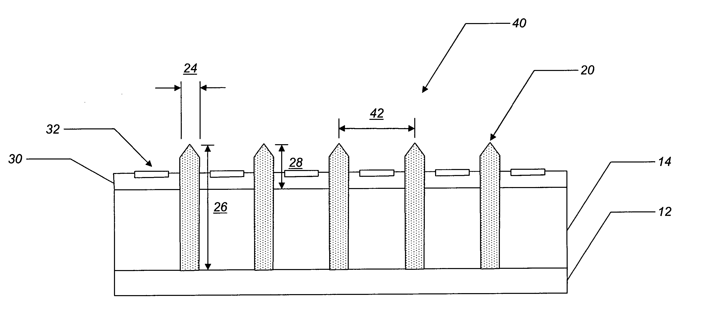
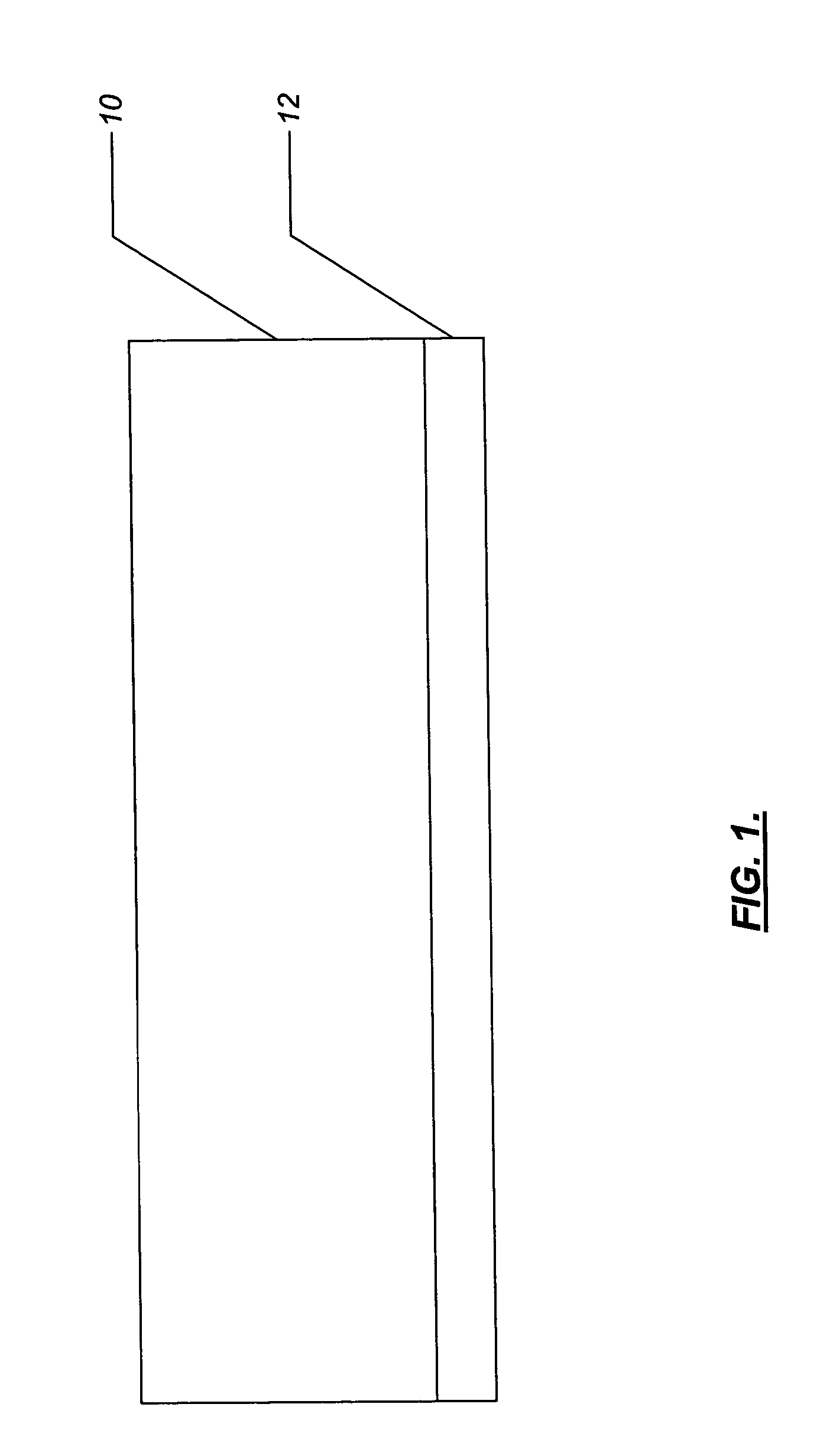
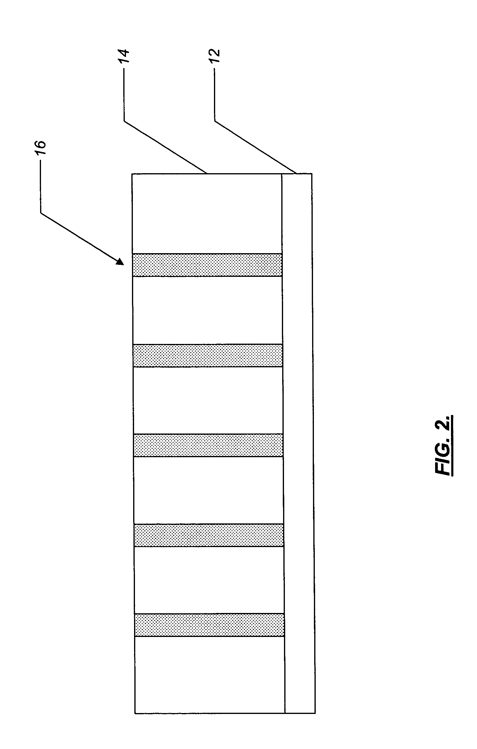
[0020] Referring to FIG. 1, in one embodiment, the method for fabricating the self-aligned gated rod field emission device of the present invention first includes depositing a metal layer 10, such as a layer of Al, Ti, Mg, W, Zn, Zr, Ta, Nb or the like, on the surface of a semiconductor layer 12, such as a layer of Si or the like, the semiconductor layer 12 forming a substrate. Preferably, the metal layer 10 has a thickness of between about 0.1 microns and about 50 microns and the semiconductor layer 12 has a thickness of between about 1 micron and about 550 microns. The metal layer 10 is deposited on the surface of the semiconductor layer 12 using, for example, thermal evaporation, electron-beam evaporation, sputtering or the like. It should be noted that Al is the preferred metal layer 10 because it may be anodically oxidized to form a nanoporous structure. There is some experimental evidence that Ti may also be anodically oxidized to form a nanoporous structure. Mg, W, Zn, Zr, Ta...


PUM


Abstract

A self-aligned gated field emission device and an associated method of fabrication are described. The device includes a substrate and a porous layer disposed adjacent to the surface of the substrate, wherein the porous layer defines a plurality of substantially cylindrical channels, each of the plurality of substantially cylindrical channels aligned substantially parallel to one another and substantially perpendicular to the surface of the substrate. The device also includes a plurality of substantially rod-shaped structures disposed within at least a portion of the plurality of substantially cylindrical channels defined by the porous layer and adjacent to the surface of the substrate, wherein a portion of each of the plurality of substantially rod-shaped structures protrudes above the surface of the porous layer. The device further includes a gate dielectric layer disposed on the surface of the porous layer, wherein the gate dielectric layer is disposed between the plurality of substantially rod-shaped structures. The device still further includes a conductive layer selectively disposed on the surface of the gate dielectric layer, wherein the conductive layer is selectively disposed between the plurality of substantially rod-shaped structures.

Description

STATEMENT REGARDING FEDERALLY SPONSORED RESEARCH AND DEVELOPMENT [0001] The present invention was made with U.S. Government support under Contract No. 70NANB2H3030, awarded by the National Institute of Standards and Technology (NIST), Department of Commerce, and the U.S. Government may therefore have certain rights in the invention.FIELD OF THE INVENTION [0002] The present invention relates generally to field emission devices that are suitable for use in x-ray imaging applications, lighting applications, flat panel field emission display applications, microwave amplifier applications, electron-beam lithography applications and the like. More specifically, the present invention relates to a self-aligned gated rod field emission device and an associated method of fabrication. BACKGROUND OF THE INVENTION [0003] Electron emission devices, such as thermionic emitters, cold cathode field emitters and the like, are currently used as electron sources in x-ray tube applications, flat panel f...

Claims


Application Information

Patent Timeline
IPC IPC(8): H01J1/304H01J3/02H01J9/02
CPCH01J1/3044H01J9/025H01J3/022
Inventor LEE, JI UNGCORDERMAN, REED ROEDERHUBER, WILLIAM HULLINGER
Owner GENERAL ELECTRIC CO
Why Eureka
Try Eureka