System and method for using first-principles simulation to provide virtual sensors that facilitate a semiconductor manufacturing process

a technology of virtual sensors and semiconductor manufacturing, applied in the field of manufacturing semiconductor devices, can solve the problems of insufficient data resolution in space and time for complete process control, material processing in the semiconductor industry presents formidable challenges, and achieves the effect of facilitating the process

Inactive Publication Date: 2005-03-31
TOKYO ELECTRON LTD
View PDF54 Cites 72 Cited by
  • Summary
  • Abstract
  • Description
  • Claims
  • Application Information

AI Technical Summary

Benefits of technology

According to another aspect of the invention, a system includes a semiconductor processing tool configured to perform a process, and an input device configured to input data relating to the process performed by the semiconductor processing tool. A first principles simulation processor is configured to input a first principles physical model relati

Problems solved by technology

Material processing in the semiconductor industry presents formidable challenges in the manufacture of integrated circuits (ICs).
The number of diagnostic systems is becoming burdensome and costly.
Yet, data sufficiently resolved in space and time for complete process control is still not available.
For example, the 2001 International Technology Roadmap for Semiconductors identifies issues impeding the development of on-tool integrated simulation capability as an enabling technology for manufacturing very small features in future semiconductor devices.
Indeed, the failure of industry to implement on-tool simulation to facilitate tool processes is primarily due to the need

Method used


Image

  • System and method for using first-principles simulation to provide virtual sensors that facilitate a semiconductor manufacturing process
  • System and method for using first-principles simulation to provide virtual sensors that facilitate a semiconductor manufacturing process
  • System and method for using first-principles simulation to provide virtual sensors that facilitate a semiconductor manufacturing process

Examples


Embodiment Construction

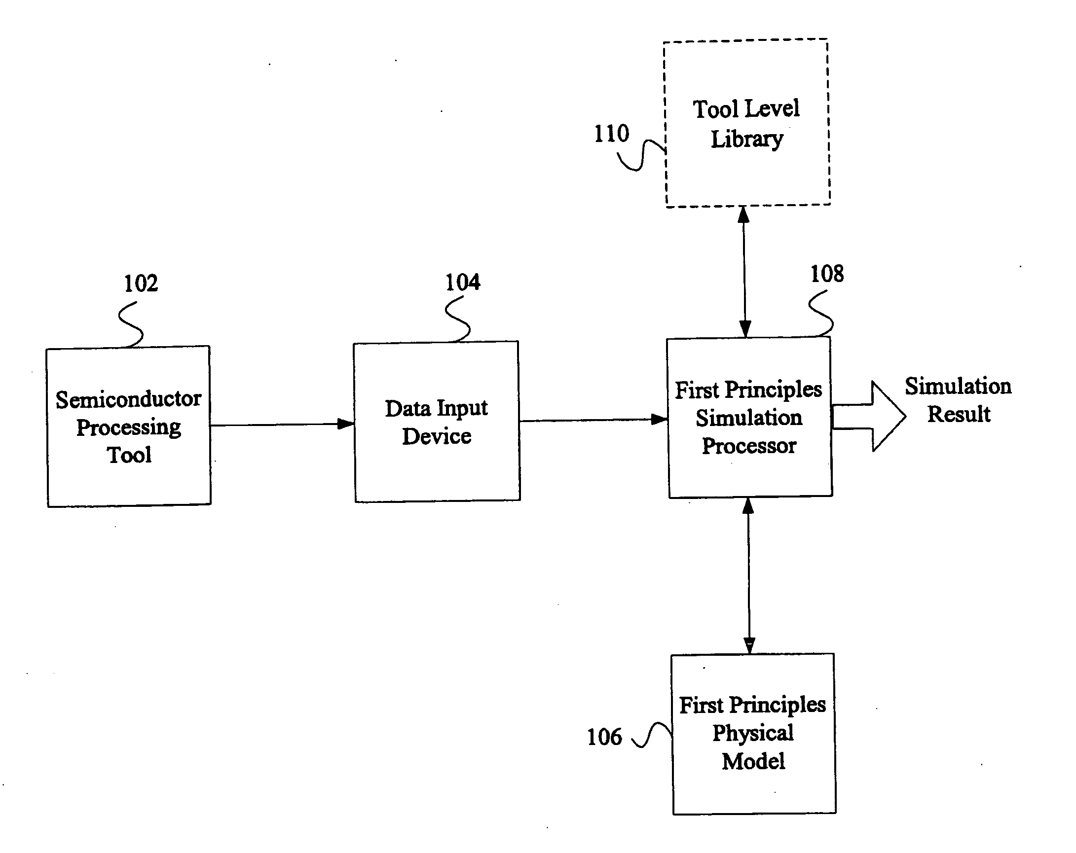
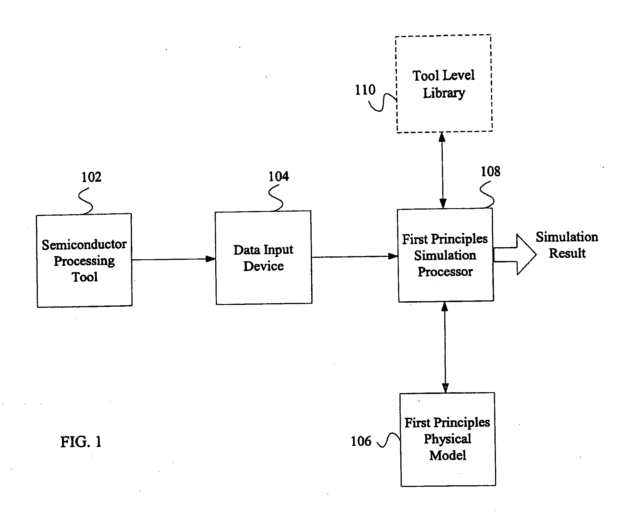
Referring now to the drawings, wherein like reference numerals designate identical or corresponding parts throughout the several views, FIG. 1 is a block diagram of a system for using first principles simulation techniques to facilitate a process performed by a semiconductor processing tool in accordance with an embodiment of the present invention. As seen in FIG. 1, the system includes a semiconductor processing tool 102, a data input device 104, a first principles physical model 106, and a first principles simulation processor 108. The system of FIG. 1 may also include a tool level library 110 as shown in phantom.

Semiconductor processing tool 102 is a tool for performing a process related to manufacturing an integrated circuit or semiconductor wafer. For example, the semiconductor processing tool 102 may be implemented as a material processing system, an etch system, a photoresist spin coating system, a lithography system, a dielectric coating system (i.e. a spin-on-glass (SOG)...


PUM


Abstract

A method, system, and computer readable medium for facilitating a process performed by a semiconductor processing tool. The method includes inputting data relating to a process performed by the semiconductor processing tool, and inputting a first principles physical model relating to the semiconductor processing tool. First principles simulation is performed using the input data and the physical model to provide a virtual sensor measurement relating to the process performed by the semiconductor processing tool, and the virtual sensor measurement is used to facilitate the process performed by the semiconductor processing tool.

Description

BACKGROUND OF THE INVENTION 1. Field of the Invention The present invention relates generally to manufacturing semiconductor devices, and more specifically to use of first principles simulation in semiconductor manufacturing processes. 2. Discussion of the Background Material processing in the semiconductor industry presents formidable challenges in the manufacture of integrated circuits (ICs). Demands for increasing the speed of ICs in general, and memory devices in particular, force semiconductor manufacturers to make devices smaller and smaller on the substrate surface. Moreover, in order to reduce fabrication costs, it is necessary to reduce the number of steps (e.g., etch steps, deposition steps, etc.) required to produce an IC structure and hence reduce the overall complexity of the IC structure and the fabrication methods thereof. These demands are further exacerbated by both the reduction in feature size and the increase of substrate size (i.e., 200 mm to 300 mm and grea...

Claims


Application Information

Patent Timeline
IPC IPC(8): G01R31/26G06F7/62G06F9/45G06F17/50H01LH01L21/66
CPCG06F17/5018G06F2217/10G06F2217/12G06F2217/80H01L2924/0002H01L22/20H01L2924/00G06F30/23G06F2111/08G06F2119/08G06F2119/18Y02P90/02G06F9/00G06F9/455H01L21/02
Inventor MITROVIC, ANDREJ S.
Owner TOKYO ELECTRON LTD
Why Eureka
Try Eureka