Germanium and germanium alloy nanoparticle and method for producing the same

a germanium alloy and nanoparticle technology, applied in the field of nanomaterials, can solve the problems of limited detection efficiency and wavelength range of bulk silicon-based photodetectors, and conventional optical detectors made on compound semiconductor substrates are bonded with bulk silicon dies for a multi-chip solution that is relatively expensive,

Inactive Publication Date: 2005-04-07
UNIV OF JORDAN THE +1
View PDF20 Cites 17 Cited by
  • Summary
  • Abstract
  • Description
  • Claims
  • Application Information

AI Technical Summary

Problems solved by technology

Conventional optical detectors made on compound semiconductor substrates are bonded with a bulk silicon die for a multi-chip solution that is relatively costly.
However, due to the large absorption length (20 μm) of silicon at 820 nm and the forbidden absorption at 1300 and 1550 nm, bulk silicon-based photodetectors have limited detection efficiency and wavelength range.

Method used


Image

  • Germanium and germanium alloy nanoparticle and method for producing the same
  • Germanium and germanium alloy nanoparticle and method for producing the same
  • Germanium and germanium alloy nanoparticle and method for producing the same

Examples


Embodiment Construction

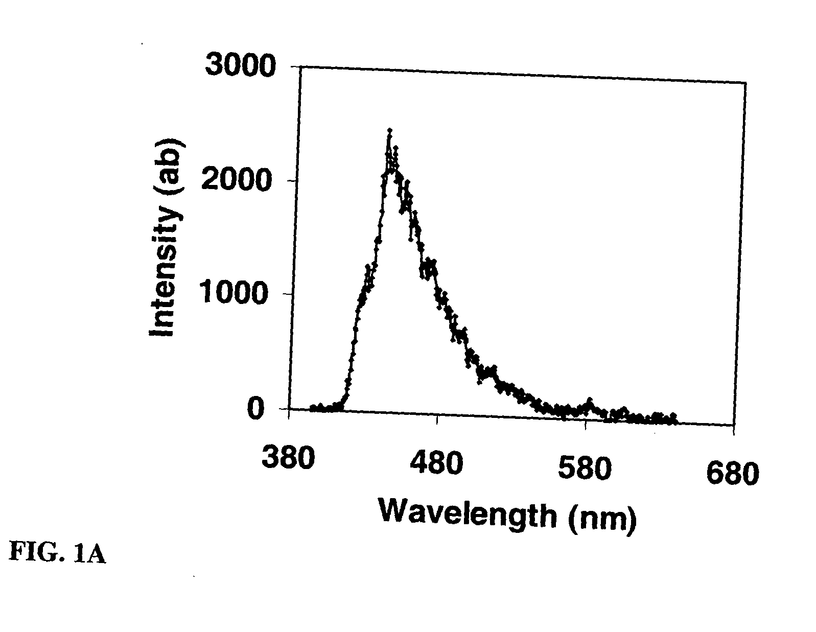
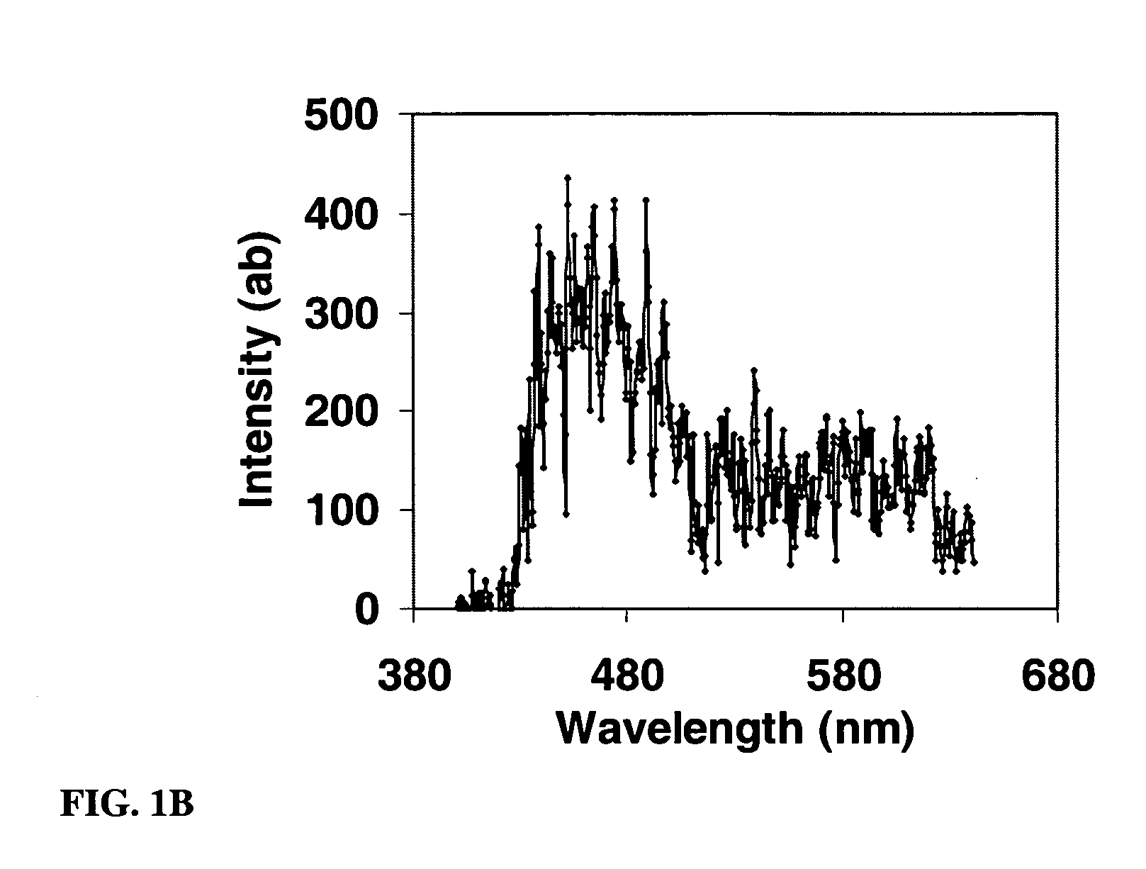
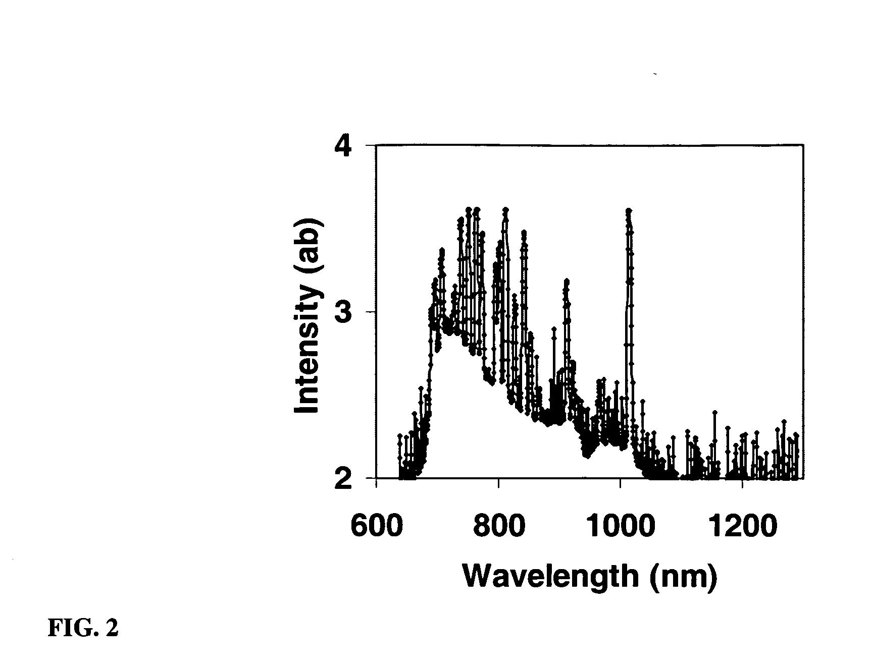
[0012] The invention concerns germanium and germanium alloy nanoparticles and methods for making the same. Infrared emissions from nanaparticles command a special interest in myriad applications. Highly-efficient nanomaterial-based photodetectors or phototransistors in the infrared can form the basis for chip-to-chip and board-to-board optical interconnects. In relation to bulk silicon, bulk germanium reduces the indirect band gap (0.66 vs. 1.1 eV), and the direct band gaps (0.9 vs. 3.2 eV), and one use of germanium nanoparticles of the invention is to extend the photosensitive response into the infrared.

[0013] In the invention, we employ electrochemical etching processes of crystalline germanium or a germanium alloy in a chemical etchant solution, e.g., HF / H2O2 / H2O to produce, well-segregated chromatic clusters of nanoparticle material, which under 365 nm UV excitation, exhibit ultrabright blue, green, and yellow / orange photoluminescence, as well as very efficient infrared radiati...


PUM

PropertyMeasurementUnit
energy gapaaaaaaaaaa
band gapaaaaaaaaaa
particle sizesaaaaaaaaaa

Abstract

In the invention, an electrochemical etching of crystalline germanium or a germanium alloy produces well-segregated chromatic clusters of nanoparticles. Distinct strong bands appear in the photoluminescence spectra under 350 nm excitation with the lowest peaks in wavelength identified to be at 430, 480, and 580 and 680-1100 nm. The material may be dispersed into a discrete set of luminescent nanoparticles of 1-3 nm in diameter, which may be prepared into colloids and reconstituted into films, crystals, etc.

Description

REFERENCE TO RELATED APPLICATIONS AND PROIRITY CLAIM [0001] This application is a continuation-in-part of co-pending application serial number 990,250, filed Nov. 21, 2001, published on Jul. 13, 2002, as publication number 20020070121 entitled FAMILY OF DISCRETELY SIZED NANOPARTICLES AND METHOD FOR PRODUCING THE SAME, which was a continuation in part of Nayfeh et al. U.S. patent application Ser. No. 09 / 426,389, entitled METHOD FOR PRODUCING SILICON NANOPARTICLES, filed Oct. 22, 1999, and now U.S. Pat. No. 6,585,947. Priority from both applications is claimed under 35 U.S.C. § 120.STATEMENT OF GOVERNMENT INTEREST [0002] This invention was made with Government assistance under contract number 1529304 awarded by the National Science Foundation. The Government has certain rights in this invention.FIELD OF THE INVENTION [0003] A field of the invention is nanomaterials. BACKGROUND OF THE INVENTION [0004] Silicon nanoparticles of ˜1 nm diameter have shown stimulated emissions. Bulk silicon...

Claims


Application Information

Patent Timeline
Patent Type & Authority Applications(United States)
IPC IPC(8): C01B33/02C25C1/22C25C5/02C25D1/00G02B6/02G02B6/10H01S3/16H01S5/04H01S5/10H01S5/30
CPCB82Y30/00C01B33/02C22B41/00C25C5/02H01S5/3031H01S5/041H01S5/10H01S5/30H01S3/163C25C1/22
Inventor NAYFEH, MUNIR H.ABUHASSAN, LAILANAYFEH, AMMAR M.CHANG, YIA-CHUNG
Owner UNIV OF JORDAN THE
Why Eureka
Try Eureka