Conductive trace structure and semiconductor package having the conductive trace structure

Active Publication Date: 2005-04-07
SILICONWARE PRECISION IND CO LTD
View PDF3 Cites 32 Cited by
  • Summary
  • Abstract
  • Description
  • Claims
  • Application Information

AI Technical Summary

Benefits of technology

[0012] The widened portions of the conductive traces at the positions across the periphery of the chip mounting area on the substrate are increased in line width to enhance the structural strength of the widened portions. As a result, in a high temperature environment, the widened portions can sustain the concentrated thermal stress from the peripheral area of

Problems solved by technology

As a result, unlike the PBGA package, the chip mounting area of the CSP cannot entirely serve as the ground paddle, making the limited surface area of the substrate 200 be in good use.
However, when the semiconductor package having the conductive traces extended out of the chip mounting area, has completed the packaging process and is subject to a high temperature environment for example in a reliability test or a reflow-soldering process during solder ball implantation, due to mismatch in coefficient of th

Method used


Image

  • Conductive trace structure and semiconductor package having the conductive trace structure
  • Conductive trace structure and semiconductor package having the conductive trace structure
  • Conductive trace structure and semiconductor package having the conductive trace structure

Examples


Embodiment Construction

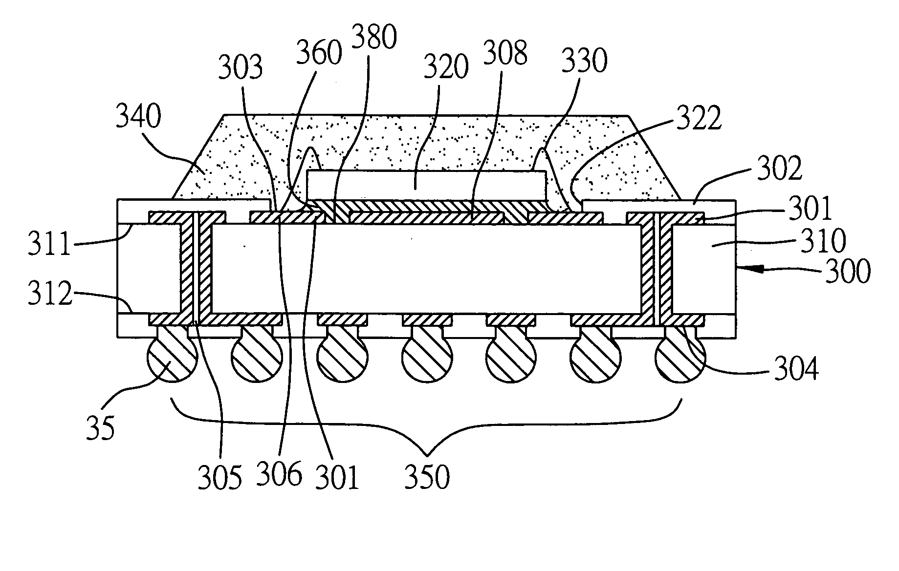
[0019] Preferred embodiments of a conductive trace structure and a semiconductor package having the conductive trace structure proposed in the present invention are described in detail as follows with reference to FIGS. 4 and 5. For the sake of simplicity, the drawings illustrate merely the elements and parts related to the embodiments of the present invention. It should be understood that the semiconductor package according to the present invention is more complex in the number of elements, the size and the entire layout in practice.

[0020] Referring to FIGS. 4 and 5, the semiconductor package having the conductive trace structure according to the present invention comprises a substrate 300, a semiconductor chip 320 mounted on a front surface 311 of the substrate 300, a plurality of bonding wires 330 such as gold wires for electrically connecting the chip 320 to the substrate 300, an encapsulation body 340 for encapsulating the chip 320, the bonding wires 330 and a part of the subs...


PUM


Abstract

A conductive trace structure and a semiconductor package having the conductive trace structure are provided. A plurality of conductive traces are formed in and surrounding a chip mounting area on a substrate, for mounting a chip on the chip mounting area. Widened portions are formed on the conductive traces in the chip mounting area and at positions across a periphery of the chip mounting area, the widened portions having a line width larger than that of the rest part of the conductive traces. The widened portions of the conductive traces can sustain concentrated thermal stress from the peripheral area of the chip caused by mismatch in coefficient of thermal expansion between the chip and the substrate. This prevents the conductive traces that pass through the periphery of the chip mounting area from cracks or breaks due to the thermal stress, thereby improving the reliability and yield of the semiconductor package.

Description

FIELD OF THE INVENTION [0001] The present invention relates to conductive trace structures and semiconductor packages having the conductive trace structures, and more particularly, to a conductive trace fabrication technology for use in a ball grid array (BGA) semiconductor package to enhance the reliability of the semiconductor package by modifying a part of the conductive trace structure. BACKGROUND OF THE INVENTION [0002] Ball grid array (BGA) packaging technology is an advanced semiconductor packaging technology, which is characterized in that a semiconductor chip is mounted on a front surface of a substrate, and a plurality of conductive elements such as solder balls are arranged in a matrix array, customarily referred to as ball grid array, on a back surface of the substrate. The ball grid array allows the semiconductor package to be bonded and electrically connected to an external printed circuit board (PCB) or other electronic devices. [0003] A typical plastic ball grid arra...

Claims


Application Information

Patent Timeline
IPC IPC(8): H01L23/498
CPCH01L23/49838H01L2224/48227H01L2924/01079H01L2924/15311H01L24/48H01L2924/01087H01L2924/07802H01L2224/45144H01L2924/00H01L24/45H01L2224/48228H01L2224/73265H01L2924/00014H01L2924/181H01L2224/05599H01L2924/00012
Inventor KUO, KUAN-TINGLAI, YU-TINGCHIANG, CHIN-CHIEN
Owner SILICONWARE PRECISION IND CO LTD
Why Eureka
Try Eureka