Manufacturing method of semiconductor device

a manufacturing method and semiconductor technology, applied in the direction of individual semiconductor device testing, semiconductor/solid-state device testing/measurement, instruments, etc., can solve the problems of difficult to cope with a product with a narrow pitch, difficult to control the height dispersion of individual bumps, and difficult to judge which portion of the bump comes in contact with the contact portion, etc., to reduce the flaws of the electrode pad, reduce the pressurizing force and damage, and reliably

Inactive Publication Date: 2005-04-07
RENESAS TECH CORP
View PDF2 Cites 3 Cited by
  • Summary
  • Abstract
  • Description
  • Claims
  • Application Information

AI Technical Summary

Benefits of technology

[0022] When many electrodes are collectively inspected, a contact method for reducing the flaws of an electrode pad at the inspecting time and reducing the pressurizing force and damage can be executed by using the above-described construction and structure. The contact can be reliably effected even in the case of plural probes and the electrode pad having an oxide film formed at several angstroms. As a result, a semiconductor element or electronic part can be very inex...

Problems solved by technology

In the structure of the bump surface described in the above-referenced publications, the inspecting contact portion of the bump surface has a large curvature, and so it is difficult to judge which portion of the bump comes in contact with the contact portion.
It is also a problem that non of these structures is easily arranged at a high density, with the result that and it is di...

Method used


Image

  • Manufacturing method of semiconductor device
  • Manufacturing method of semiconductor device
  • Manufacturing method of semiconductor device

Examples


Embodiment Construction

[0036] The embodiments of the present invention will be explained with reference to FIGS. 1 to 12.

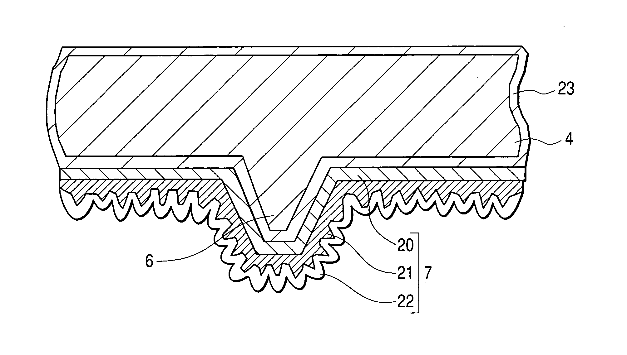
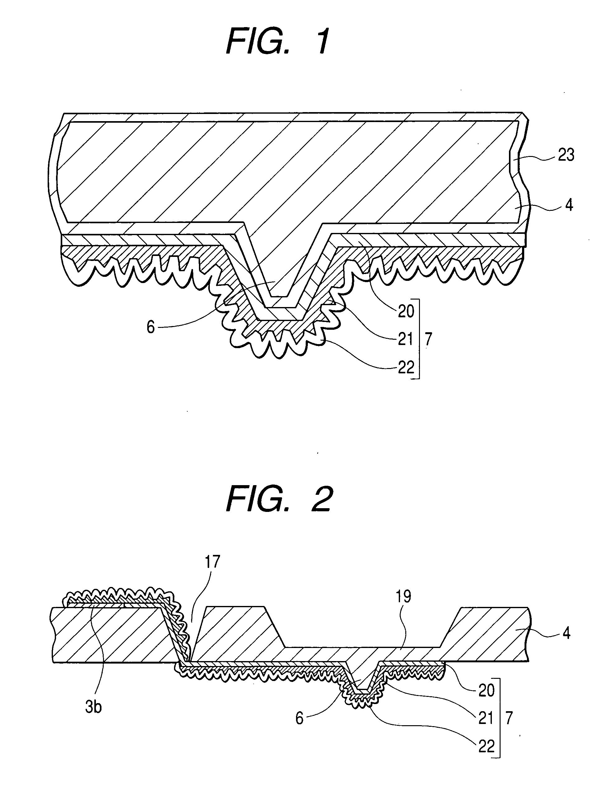
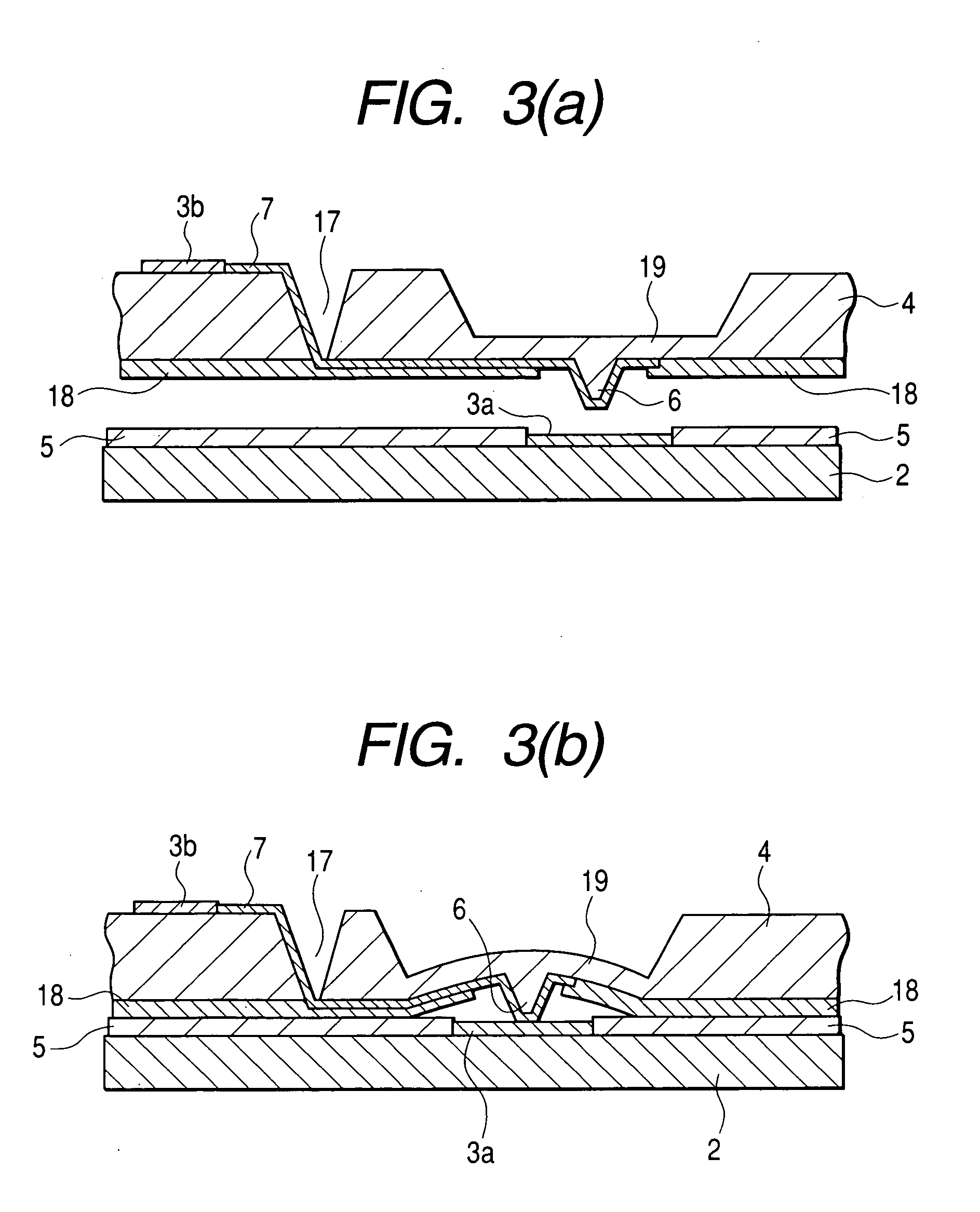
[0037]FIG. 1 shows a typical example of the present invention. FIG. 1 is an enlarged sectional view of one portion of a substrate for use in semiconductor inspection to detect a defect in a semiconductor device. A probe 6 is formed in the substrate 4 for an inspection, and its circumference is covered with an insulating layer 23. A multi-layer wiring 7 is formed on one principal surface of this substrate 4. The multi-layer wiring 7 is formed in the order of a close attaching layer 20, a foundation layer 21 and an electrically conductive layer 22, arranged from the substrate surface side. The close attaching layer is provided to improve the close attaching property of an insulating layer and the close attaching layer. For example, when silicon dioxide is used in the insulating layer, titanium and gold are formed in the close attaching layer.

[0038] Irregularities having a crest interval...


PUM


Abstract

A manufacturing method for improving the yield in a semiconductor manufacturing process and reducing the manufacturing cost produces a semiconductor device that is inexpensively manufactured and has a high reliability by reliably making contact during inspection with a suitable pressing force, while limiting damage to an electrode pad even when many inspected electrodes are inspected. A substrate used for inspection of the semiconductor device has a beam, a probe on the beam having a projecting shape for coming in contact with an electrode (electrode pad) of the semiconductor device, and a secondary electrode electrically connected to the probe through an electrically conductive member disposed on the side of the beam opposed to the side where the probe is provided. In an inspecting process, an inspecting device having a layer having many projections formed in the probe come in contact with the electrode pad of the semiconductor device.

Description

BACKGROUND OF THE INVENTION [0001] The present invention relates to a method of manufacture of a semiconductor device; and, more particularly, the invention relates to a technique for making an electrical connection from an inspecting device to a semiconductor device, that is formed in a semiconductor substrate, so as to carry out an inspection of the semiconductor device during the manufacture thereof. [0002] A method of manufacture of a semiconductor device, such as an IC, an LSI, etc., is generally divided into a so-called pre-process, which includes steps carried out up to the formation of an integrated circuit on the surface of a silicon wafer, and a so-called after-process, which includes steps during which this silicon wafer is cut and separated into individual chips and is sealed by resin, ceramic, etc. In these semiconductor devices, the electrical characteristics of each circuit are inspected, and non-defective and defective products (chips) are judged in a chip unit at a ...

Claims


Application Information

Patent Timeline
IPC IPC(8): G01R31/26G01R1/067G01R1/073G01R3/00H01L21/66
CPCG01R1/06761G01R3/00G01R1/0735
Inventor KANAMARU, MASATOSHIAONO, TAKANORINAGATA, TATSUYAKAWAKAMI, KENJIAOKI, HIDEYUKI
Owner RENESAS TECH CORP
Why Eureka
Try Eureka