Organic light emitting device, manufacturing method thereof, and display unit

a technology of light emitting device and display unit, which is applied in the direction of static indicating device, discharge tube luminescnet screen, instruments, etc., can solve the problems of auxiliary wiring b>, second electrode b>, and difficult to form organic layer, so as to improve process yield, inhibit the effect of screen luminance variation and improving display quality

Inactive Publication Date: 2005-04-14
THOMSON LICENSING SA
View PDF10 Cites 95 Cited by
  • Summary
  • Abstract
  • Description
  • Claims
  • Application Information

AI Technical Summary

Benefits of technology

According to the organic light emitting device of the invention and the display unit of the invention, the organic layer has the break part at the side face of the auxiliary wiring, and the auxiliary wiring and the second electrode are electrically connected through this break part. Therefore, voltage drop in the second electrode is inhibited by the auxiliary wiring, and variation of luminance in the screen can be inhibited. Consequently, a display quality can be improved.
According to the method of manufacturing an organic light emitting device of the invention, after the break part is formed by breaking the organic layer by the step of the side face of the auxiliary wiring, the second electrode and the auxiliary wiring are electrically connected through this break part. Therefore, even when the organic layer is formed without using a mask for pixel coating, the auxiliary wiring and the second electrode can be electrically connected. Consequently, deposition failure such as lack of the organic layer due to displacement or influence of thermal expansion of the mask for pixel coating can be prevented to improve process yield, which is significantly advantageous for making a high-definition display. Further, it is possible to prevent dust and the like adhering to the mask for pixel coating from adhering to the organic layer and the like, which leads to a cause of short circuit. Furthermore, no extra process is needed to electrically connect the second electrode and the auxiliary wiring. Therefore, the number of processes can be less.

Problems solved by technology

However, when a high-definition organic light emitting display is fabricated, it is hard to form the organic layer 112 precisely due to influence of thermal expansion of the mask for pixel coating 120.
This leads to a problem that the auxiliary wiring 113A and the second electrode 113 cannot be electrically connected.

Method used


Image

  • Organic light emitting device, manufacturing method thereof, and display unit
  • Organic light emitting device, manufacturing method thereof, and display unit
  • Organic light emitting device, manufacturing method thereof, and display unit

Examples


first embodiment

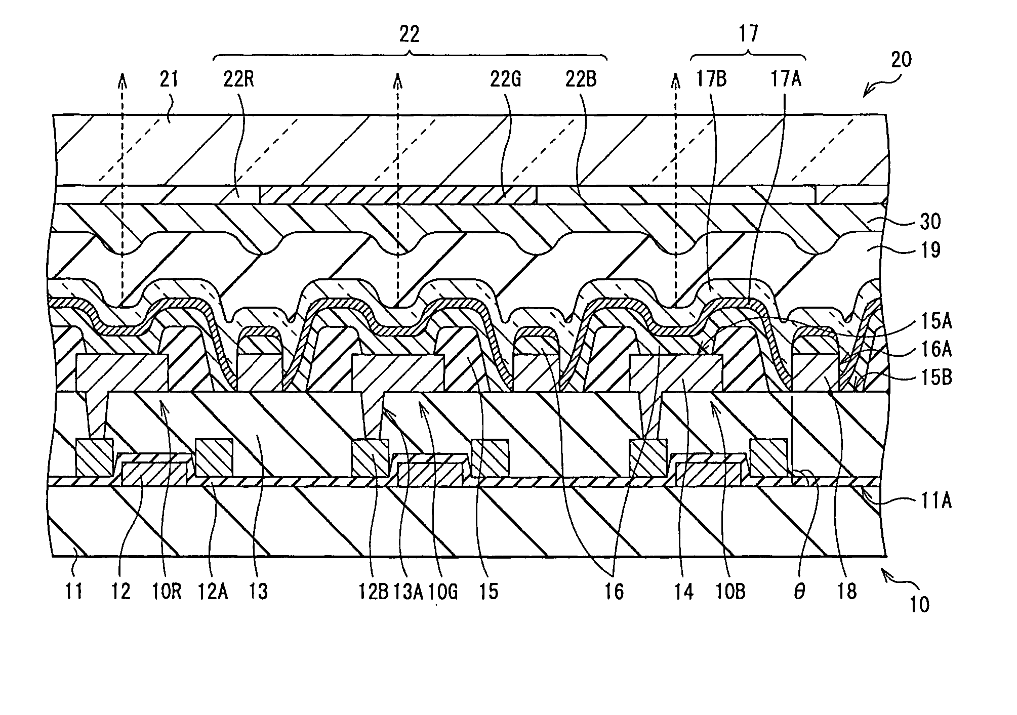
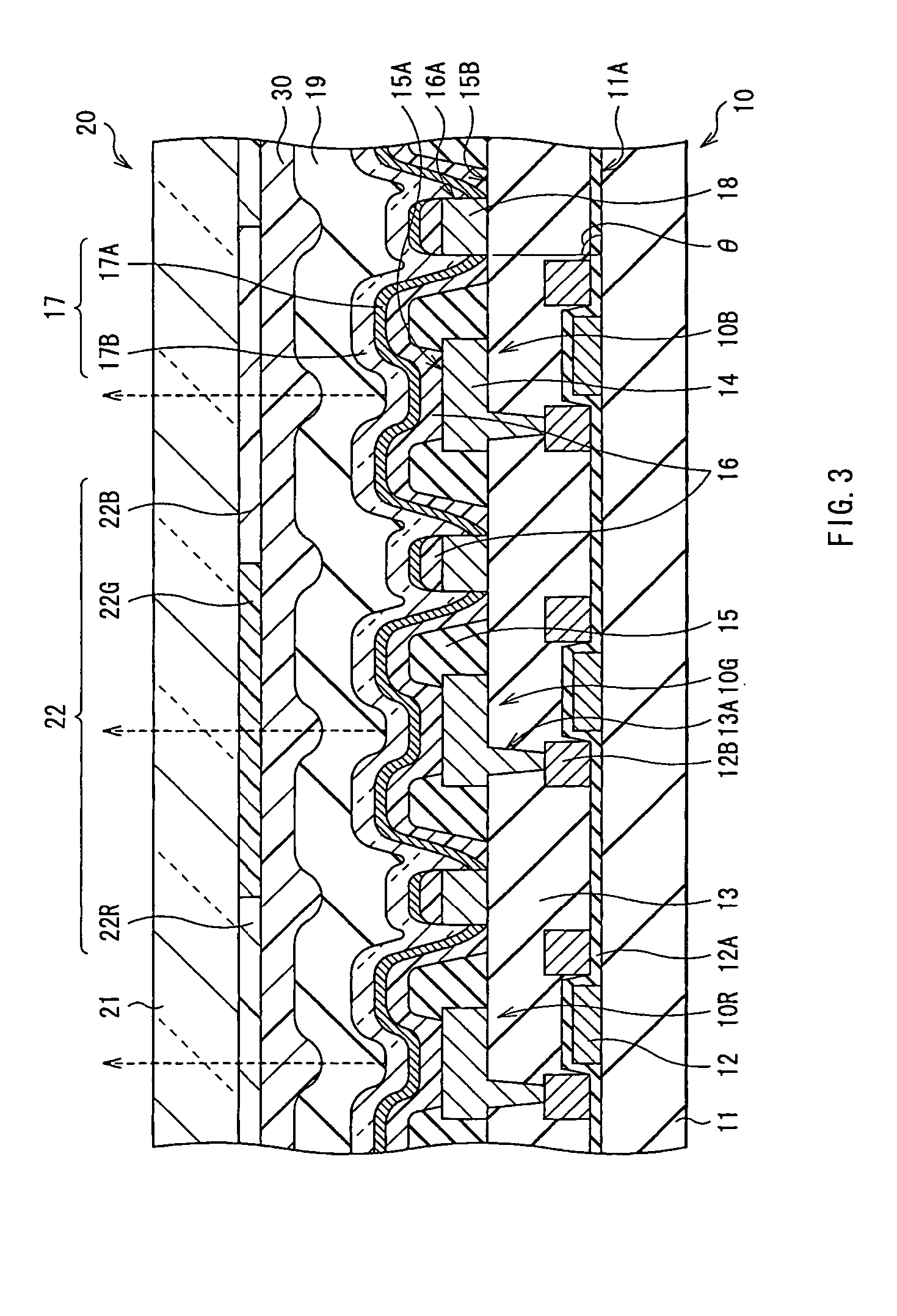
FIG. 3 shows a cross sectional structure of a display unit according to a first embodiment of the invention. This display unit is used as an ultrathin organic light emitting display, wherein a driving panel 10 and a sealing panel 20 are placed opposite, and their whole surfaces are bonded together by an adhesive layer 30 made of, for example, a thermosetting resin. The driving panel 10 is, for example, sequentially provided with an organic light emitting device 10R generating red light, an organic light emitting device 10G generating green light, and an organic light emitting device 10B generating blue light in the shape of a matrix as a whole on a substrate 11 made of an insulating material such as glass with a TFT 12 and a planarizing layer 13 in between.

The TFT 12 is an active device corresponding to the respective organic light emitting devices 10R, 10G, and 10B. The organic light emitting devices 10R, 10G, and 10B are driven by active matrix method. A gate electrode of the TF...

second embodiment

FIG. 13 shows a cross sectional structure of a display unit according to a second embodiment. This display unit is the same as the display unit of the foregoing first embodiment except that an auxiliary wiring 68 is provided on the insulating film 15. Therefore, the same symbols are applied to the same components as of the first embodiment and explanation thereof will be omitted.

The auxiliary wiring 68 has a monolayer structure or a laminated structure of a low resistance conductive material such as aluminum (Al) and chromium (Cr). A width and a thickness of the auxiliary wiring 68 vary according to dimensions of a screen, materials and thicknesses of the second electrode and the like. In this embodiment, the auxiliary wiring 68 can have a different construction from that of the first electrode 14, and the construction of the auxiliary wiring 68 is not bound by a material or a thickness of the first electrode 14. Therefore, for example, it is possible to lower a sheet resistance o...


PUM


Abstract

The invention provides an organic light emitting device which can electrically connect an auxiliary wiring and a second electrode without using a mask for pixel coating, a manufacturing method thereof, and a display unit. In organic light emitting devices, for example, a first electrode as an anode, an insulating film, an organic layer including a light emitting layer, and a second electrode as a cathode are layered in this order from a substrate side. The organic layer has a break part on a side face of an auxiliary wiring. The auxiliary wiring and the second electrode are electrically connected through this break part.

Description

BACKGROUND OF THE INVENTION 1. Field of the Invention The present invention relates to an organic light emitting device comprising an auxiliary wiring between pixels, a manufacturing method thereof, and a display unit using it. 2. Description of the Related Art In these years, as one of flat panel displays, an organic light emitting display which uses organic light emitting devices has been noted. The organic light emitting display has characteristics that its visual field angle is wide and its power consumption is low since it is a self-luminous type display. The organic light emitting display is also thought of as a display having sufficient response to high-definition high-speed video signals, and is under development toward the practical use. As an organic light emitting device, for example, as shown in FIG. 1, an organic light emitting device, wherein a first electrode 111, an organic layer 112 including a light emitting layer, and a second electrode 113 are sequentially l...

Claims


Application Information

Patent Timeline
Patent Type & Authority Applications(United States)
IPC IPC(8): H05B33/26G09G3/30H01L27/32H01L51/50H01L51/52H05B33/00H05B33/10H05B33/12H05B33/14H05B33/22H05B44/00
CPCH01L27/3246H01L51/5036H01L2251/5315H01L51/5228H01L51/5234H01L51/5218H10K59/122H10K50/125H10K50/818H10K50/824H10K50/828H10K2102/3026H10K59/80522H05B33/00H05B33/26H05B33/10
Inventor YAMADA, HIROKAZUHIRANO, TAKASHIHANAWA, KOHJI
Owner THOMSON LICENSING SA
Why Eureka
Try Eureka