Laminated low pass filter
a low-pass filter and laminate technology, applied in waveguide devices, waveguide type devices, electrical equipment, etc., can solve the problems of complex manufacturing of laminated low-pass filters, degraded insertion loss characteristics, and difficult to manage respective characteristics of filters used in filters, etc., to achieve the effect of improving insertion loss characteristics and minimizing siz
- Summary
- Abstract
- Description
- Claims
- Application Information
AI Technical Summary
Benefits of technology
Problems solved by technology
Method used
Image
Examples
first embodiment
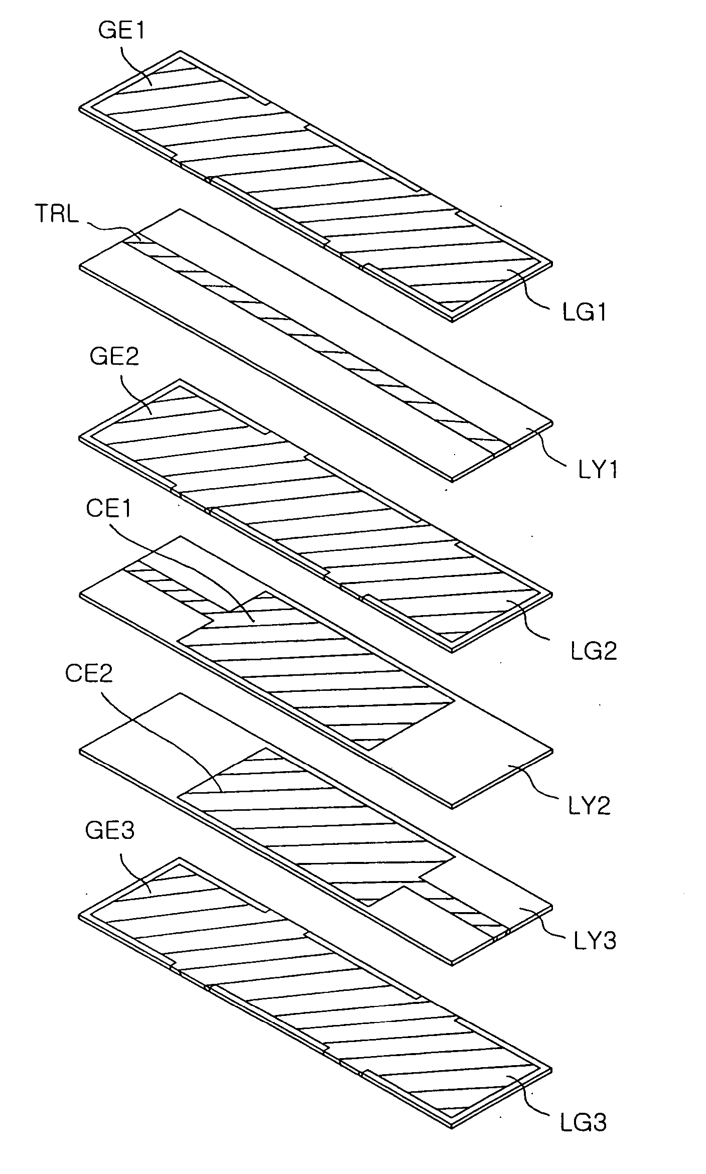
[0045]FIG. 6 is a perspective view illustrating a laminated structure of the laminated low pass filter according to the present invention.
[0046] In the case of FIG. 6, the capacitor electrode structure includes a first capacitor electrode CE1 formed on the second dielectric layer LY2 arranged beneath the first dielectric layer LY1, and connected at one end thereof to the input electrode IN, and a second capacitor electrode CE2 formed on the third dielectric layer LY3 arranged beneath the second dielectric layer LY2 such that a capacitance C is formed between the first and second capacitor electrodes CE1 and CE2.
[0047] The laminated low pass filter also includes a first ground electrode GE1, a second ground electrode GE2, and a third ground electrode GE3. The first ground electrode GE1 is formed on a first ground layer LG1 laminated over the first dielectric layer LY1 at one side of the first ground layer LG1. The first ground electrode GE1 is connected with an associated one of the...
second embodiment
[0048]FIG. 7 is a perspective view illustrating a laminated structure of the laminated low pass filter according to the present invention.
[0049] In the case of FIG. 7, the capacitor electrode structure includes a first capacitor electrode CE1 formed on the second dielectric layer LY2 arranged beneath the first dielectric layer LY1, and a second capacitor electrode CE2 formed on the third dielectric layer LY3 arranged beneath the second dielectric layer LY2 such that a capacitance C is formed between the first and second capacitor electrodes CE1 and CE2. The second capacitor electrode CE2 includes a capacitor electrode CE2A formed on the third dielectric layer LY3 at one side of the third dielectric layer LY3, and connected at one end thereof to the input electrode IN, and a capacitor electrode CE2B formed on the third dielectric layer LY3 at the other side of the third dielectric layer LY3 in such a manner that it is separate from the capacitor electrode CE2A, while being connected ...
PUM
 Abstract
Description
Claims
Application Information


