Low noise image sensing system and method for use with sensors with very small pixel size

a sensor and low noise technology, applied in the field of solid state image sensors, can solve the problems of direct relationship between chip size and consequently pixel size, obstacles and limitations in the process that need to be overcome first, and the small well capacity of smaller pixels, so as to achieve small pixel sizes, small well capacity, and high performance.

Active Publication Date: 2005-04-14
TEXAS INSTR INC
View PDF8 Cites 37 Cited by
  • Summary
  • Abstract
  • Description
  • Claims
  • Application Information

AI Technical Summary

Benefits of technology

[0003] It is an object of the present invention to overcome limitations in prior art. It is further object of the present invention to provide a practical design of image sensing system that uses sensors with very small p

Problems solved by technology

The cost can be directly related to chip size and consequently to the pixel size.
There are, however, some obstacles and limitations in this process that need to be overcome first.
However, smaller pixels also have a small well capacity and

Method used


Image

  • Low noise image sensing system and method for use with sensors with very small pixel size
  • Low noise image sensing system and method for use with sensors with very small pixel size

Examples


Embodiment Construction

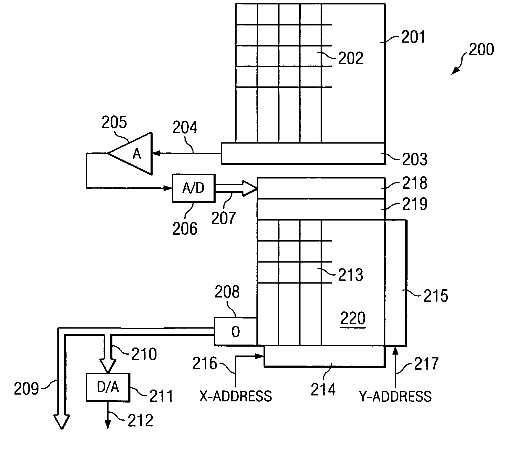
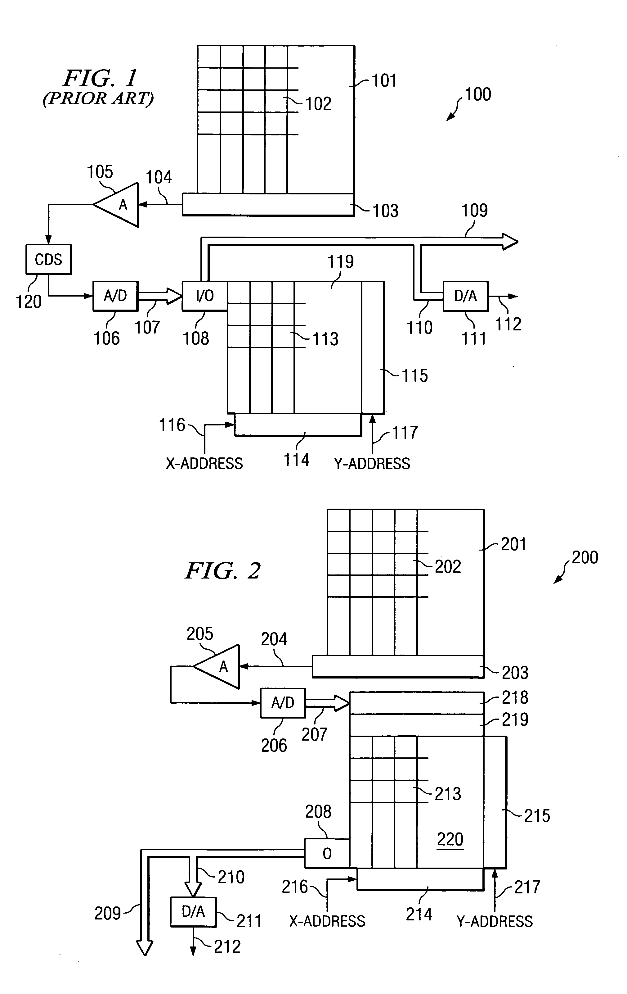
[0008] In FIG. 1 drawing 100 represents a simplified block diagram of a typical prior art image sensing system that consists of array of pixels 101. When light impinges on the array charge is produced in individual pixels 102 and is integrated there. After completion of integration cycle, charge is readout first by shifting the whole line of pixels 102 into serial register 103 and then by shifting individual pixels one-by-one into charge detection node 104 that is buffered by amplifier 105. It is clear to those skilled in the art that CCD image area pixel array 101 can be easily replaced by a CMOS area pixel array and the readout register 103, detection node 104, and buffer amplifier 105, replaced by corresponding CMOS scanning and addressing circuits. For the simplicity of description such an alternative will not be discussed here any further. When the pixels of CMOS array are reset or when charge detection node 104 of the CCD image sensor is reset kTC noise is generated. This nois...


PUM


Abstract

The image sensing system includes integrating charge in an image sensor array; transferring the charge out of the image sensor array; converting the charge to a digital signal; combining the digital signal with digital data stored in a memory device to form an integrated signal; storing the integrated signal in the memory device such that the integrated signal becomes the digital data; and repeating the above steps multiple times during a frame time cycle. This system allows for very small pixel sizes in the image sensor. The digital integration process eliminates the need for using correlated double sampling circuits to reduce kTC noise, and is also beneficial for reduction of analog-to-digital digitization noise.

Description

FIELD OF THE INVENTION [0001] The present invention relates to solid-state image sensors and specifically to CMOS and CCD image sensors that have very small pixel sizes. BACKGROUND OF THE INVENTION [0002] A typical image sensor senses light by converting impinging photons into electrons that are integrated (collected) in the image sensing area array of pixels. After completion of integration collected electrons are transported into a suitable storage area by the CCD transfer process and further from the storage area into the detection node where electron signal charge is converted into a voltage. The resulting voltage is then supplied to the output terminals of the sensor. In CMOS image sensors; charge is converted into a voltage directly in the pixels themselves without any transport and the resulting voltage, after appropriate buffering, is delivered to the output terminals through various scanning and addressing means. The description of a CCD image sensor can be found for exampl...

Claims


Application Information

Patent Timeline
IPC IPC(8): H04N5/363H04N5/369
CPCH04N5/3355H04N25/772
Inventor HYNECEK, JAROSLAV
Owner TEXAS INSTR INC
Why Eureka
Try Eureka