

Method for producing an electrically conductive contact
- Summary
- Abstract
- Description
- Claims
- Application Information
AI Technical Summary
Benefits of technology
Problems solved by technology
Method used
Image

Examples
first embodiment
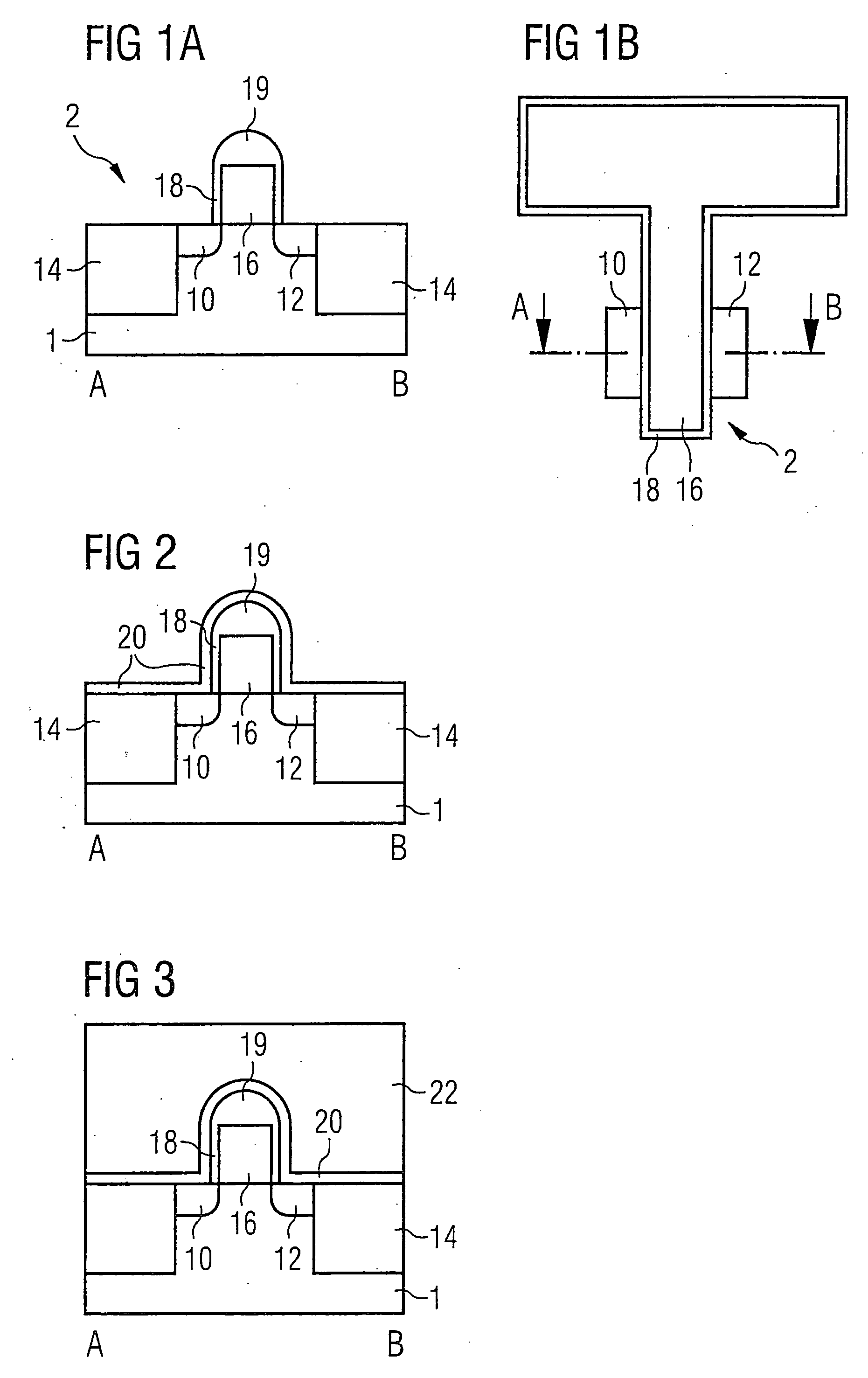
[0076] The cross-sectional profiles shown reproduce a sequence of process steps according to the invention in accordance with the abovementioned FIG. 1a shows a cross-sectional profile and FIG. 1b a plan view of a field-effect transistor 2 in an initial situation for the method. The field-effect transistor 2 is formed in the substrate 1 and comprises a first doped region 10, a second doped region 12, a word line or gate 16 with a pad terminal depicted only by way of example, an all-round insulation comprising lateral oxide spacers 18 and a nitride cover 19, and also a shallow trench isolation (STI) 14. The cross-sectional profile shown in FIG. 1a is shown along a line A-B in the plan view of FIG. 1b.
[0077] In a conformal deposition process, a liner 20 made of silicon dioxide is deposited onto the surface of these structures (FIG. 2). The liner 20 preferably has a thickness of about 15 nm. The width of the word line 16 is about 140 nm. The oxide spacer 18 has a thickness of 6 nm, w...
sixth embodiment
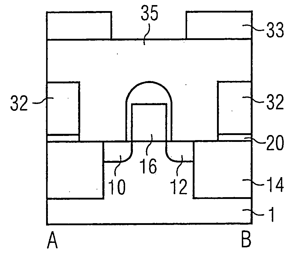
[0090] A further exemplary embodiment corresponding to the sixth embodiment is shown in FIGS. 17 to 20. A contact-connection to a field-effect transistor with uniform metallization material for the contact and interconnect region without any interface between the two regions is produced in the case of this example. A damascene patterning is employed here. Two mask and three planarization steps are used.
[0091] The starting point is the state illustrated in FIG. 6, i.e., the steps shown in FIGS. 1-6 are firstly to be employed in this case, too. FIG. 17 shows the deposition of a dielectric layer for forming the interlevel insulator 32. A resist 33 is applied to the surface, which, although it is planarized, is not planarized back therein to the polysilicon plugs of the first conductive layer 22, and said resist is exposed outside a region above the ridge in a mask step (FIG. 18). In an anisotropic etching, the exposed regions are transferred into the interlevel insulator 32 until the f...
seventh embodiment
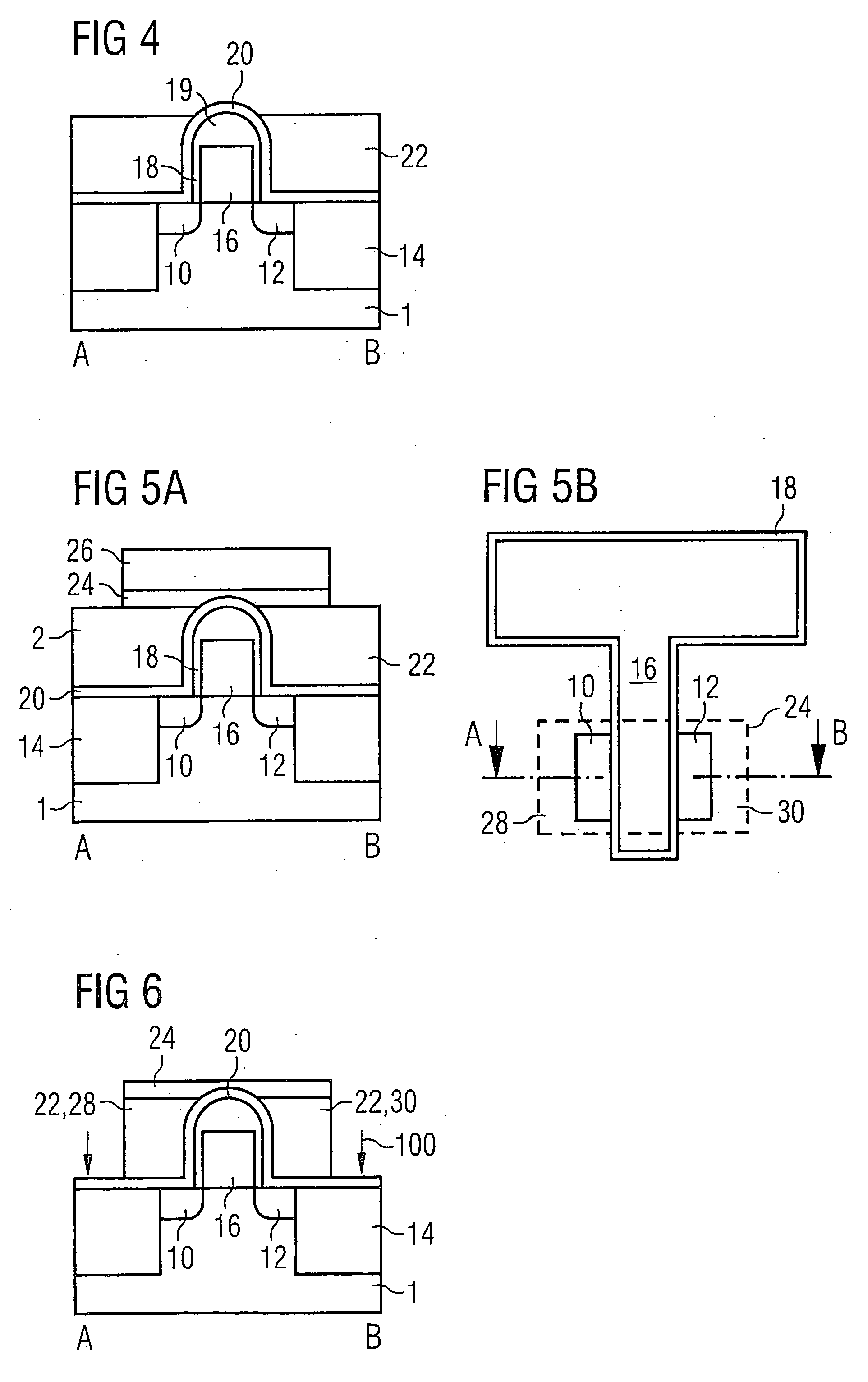
[0093] A further, fourth exemplary embodiment is shown in FIGS. 21 to 26. It represents an example of the What is produced in this case is a contact-connection to an individual field-effect transistor with a uniform metallization material for the contact plug and interconnect region, i.e., without the formation of a contact interface between the two regions. The interconnects are realized by means of dual damascene patterning in this case. The production requires three mask steps and three planarization steps (CMP).
[0094] In contrast to the third exemplary embodiment, the process is continued starting from the state shown in FIG. 17 in the case of that in FIG. 21, i.e., the order of the process steps is reproduced by FIGS. 1-6, 17, 21-26.
[0095] In a further mask step—as is shown in FIG. 21—a resist 33 deposited on the planarized dielectric layer as an interlevel insulator is exposed in such a way that a respective opening is realized for each of the two partial regions 28, 30. The...
PUM
 Abstract
Description
Claims
Application Information