Stacked semiconductor device and semiconductor chip control method

a technology of semiconductor chips and control methods, applied in semiconductor devices, digital storage, instruments, etc., can solve the problems of plurality of chips performing the same operation, increase in the size of chips associated with improvements in the functions of lsi chips, and inability to prevent process-based miniaturization

Inactive Publication Date: 2005-04-21
ELPIDA MEMORY INC
View PDF8 Cites 266 Cited by
  • Summary
  • Abstract
  • Description
  • Claims
  • Application Information

AI Technical Summary

Benefits of technology

[0028] It is an object of the present invention to provide a semiconductor device which can employ a plurality of semiconductor chips in the same design that are stacked one upon another,

Problems solved by technology

It is anticipated that if the semiconductor manufacturing process encounters difficulties in miniatualization in the future, an increase in the size of chips associated with improvements on functions of LSI chips (for example, an increased storage capacity of DRAM) cannot be prevented by process-based miniatualization.
This can cause a problem that the plurality of chips performs the same operation.
It is said, however, that if the blind throughhole structure is formed using a refractory metal such as titanium, tungsten or the like or a compound thereof in a chip which is manufactured using high-temperature processes, the resulting chip will not lend itself to micro-machining by dry etching, and will also imply a problem of corrosion after the et

Method used


Image

  • Stacked semiconductor device and semiconductor chip control method
  • Stacked semiconductor device and semiconductor chip control method
  • Stacked semiconductor device and semiconductor chip control method

Examples


first embodiment

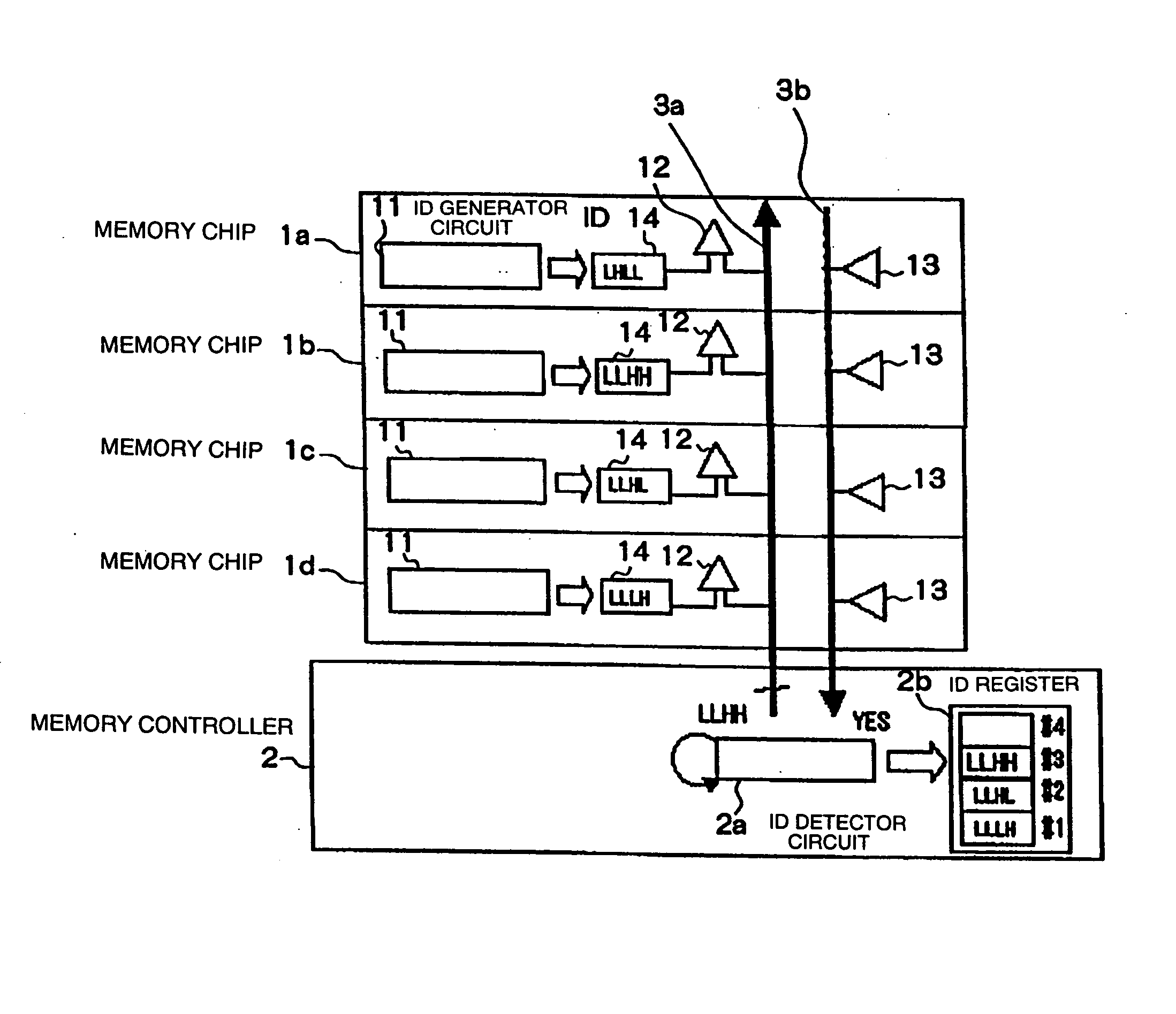
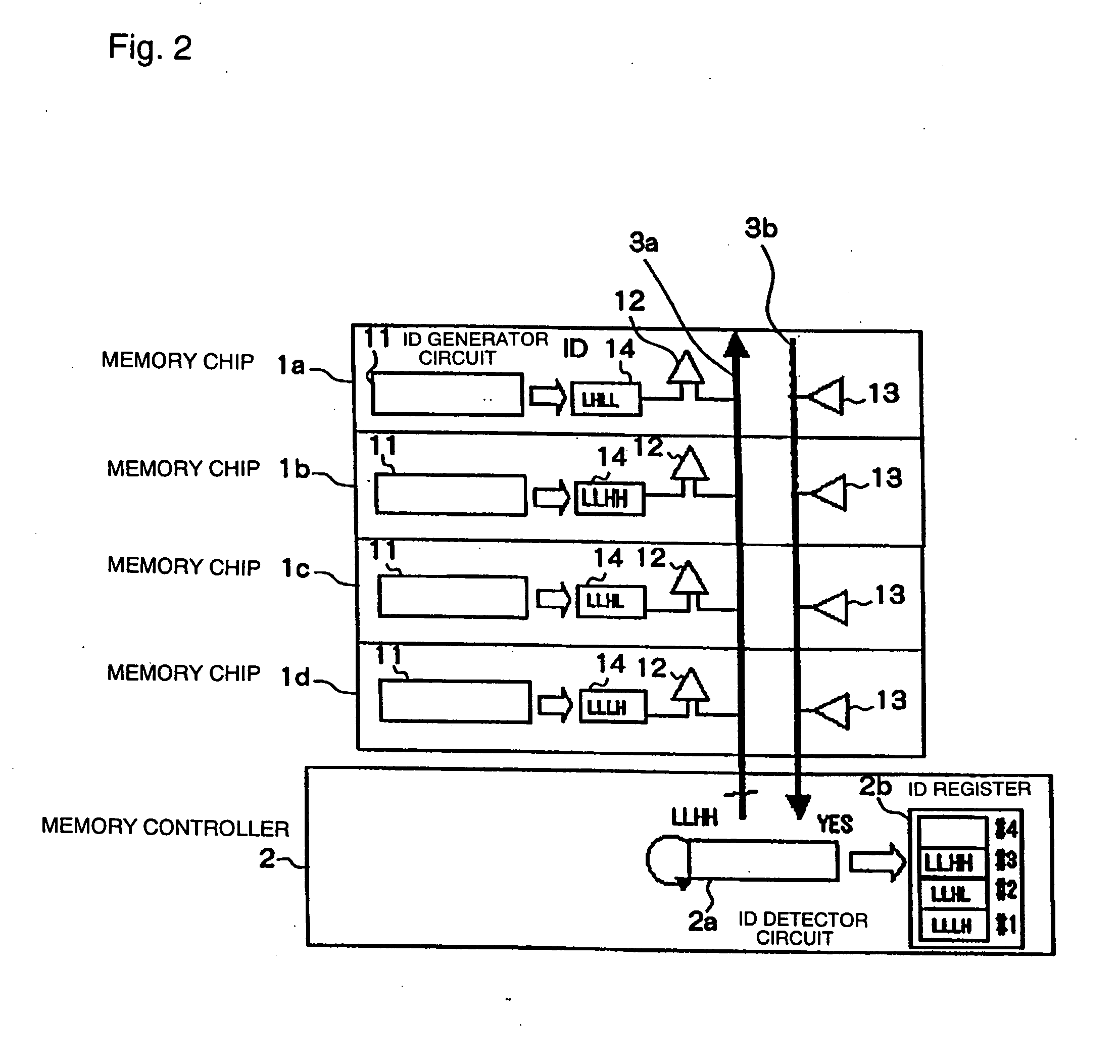
[0107]FIG. 3 is a block diagram illustrating ID generator circuit 1 shown in FIG. 2. In FIG. 3, components identical to those shown in FIG. 2 are designated with the same reference numerals.

[0108] In FIG. 3, ID generator circuit 11a includes ring oscillator (self-running oscillator) 11a1, timer 11a2, counter 11a3, and selector 11a4. Ring oscillator 11a1 generates a high frequency signal (at a pulse period of several ns). Ring oscillator 11a1 includes a plurality of transistors 11a1a. Timer 11a2 generates a time-up signal at intervals of several microseconds. Counter 11a3 counts the number of pulses delivered from ring oscillator 11a1. Selector 11a4, responsive to the time-up signal generated by timer 11a2, forces ring oscillator 11a1 to stop supplying its output to counter 11a3, thereby stopping the counting of counter 11a3.

[0109] ID generator circuit 11a defines ID 14 as indicated by the counted value on counter 11a3 at this time.

[0110] Each of the stacked memory chips 1a-1d can ...


PUM


Abstract

Each of stacked memory chips has an ID generator circuit for generating identification information in accordance with its manufacturing process. Since the memory chip manufacturing process implies process variations, the IDs generated by the respective ID generator circuits are different from one another even though the ID generator circuits are identical in design. A memory controller instructs an ID detector circuit to detect the IDs of the respective memory chips, and individually controls the respective memory chips based on the detected IDs.

Description

BACKGROUND OF THE INVENTION [0001] 1. Field of the Invention [0002] The present invention relates to a semiconductor device and a semiconductor chip control method, and more particularly, to a stacked semiconductor device which has semiconductor chips such as memory chips stacked one upon another, and a method of controlling such semiconductor chips. [0003] 2. Description of the Related Art [0004] It is anticipated that if the semiconductor manufacturing process encounters difficulties in miniatualization in the future, an increase in the size of chips associated with improvements on functions of LSI chips (for example, an increased storage capacity of DRAM) cannot be prevented by process-based miniatualization. [0005] To cope with such a possible problem, a CoC (Chip on Chip) structure has been devised for semiconductor devices (for example, DRAM) which may includes LSI chips stacked one upon another for three-dimensionally expanding functions of the LSI chips (for example, the sto...

Claims


Application Information

Patent Timeline
IPC IPC(8): G11C11/408G11C5/06G11C8/12G11C11/401G11C11/407G11C11/413H01L23/495H01L23/544H01L25/00H01L25/065H01L25/18
CPCH01L23/544H01L25/0657H01L25/18H01L2223/5444H01L2224/16H01L2225/06527H01L2225/06572H01L2924/15311H01L2924/15331H01L2225/06513
Inventor FUNABA, SEIJINISHIO, YOJI
Owner ELPIDA MEMORY INC
Why Eureka
Try Eureka