

Measurement techniques for controlling aspects of a electroless deposition process
a technology of electroless deposition and measurement techniques, applied in the direction of liquid/solution decomposition chemical coatings, coatings, chemistry apparatuses and processes, etc., can solve the problems of difficult to know when the desired thickness of material has been deposited across the surface of the substrate, the difficulty of filling void-free interconnect feature filling via conventional metallization techniques, and the difficulty of accurately controlling conventional processing apparatuses and methods
- Summary
- Abstract
- Description
- Claims
- Application Information
AI Technical Summary
Benefits of technology
Problems solved by technology
Method used
Image

Examples
Embodiment Construction
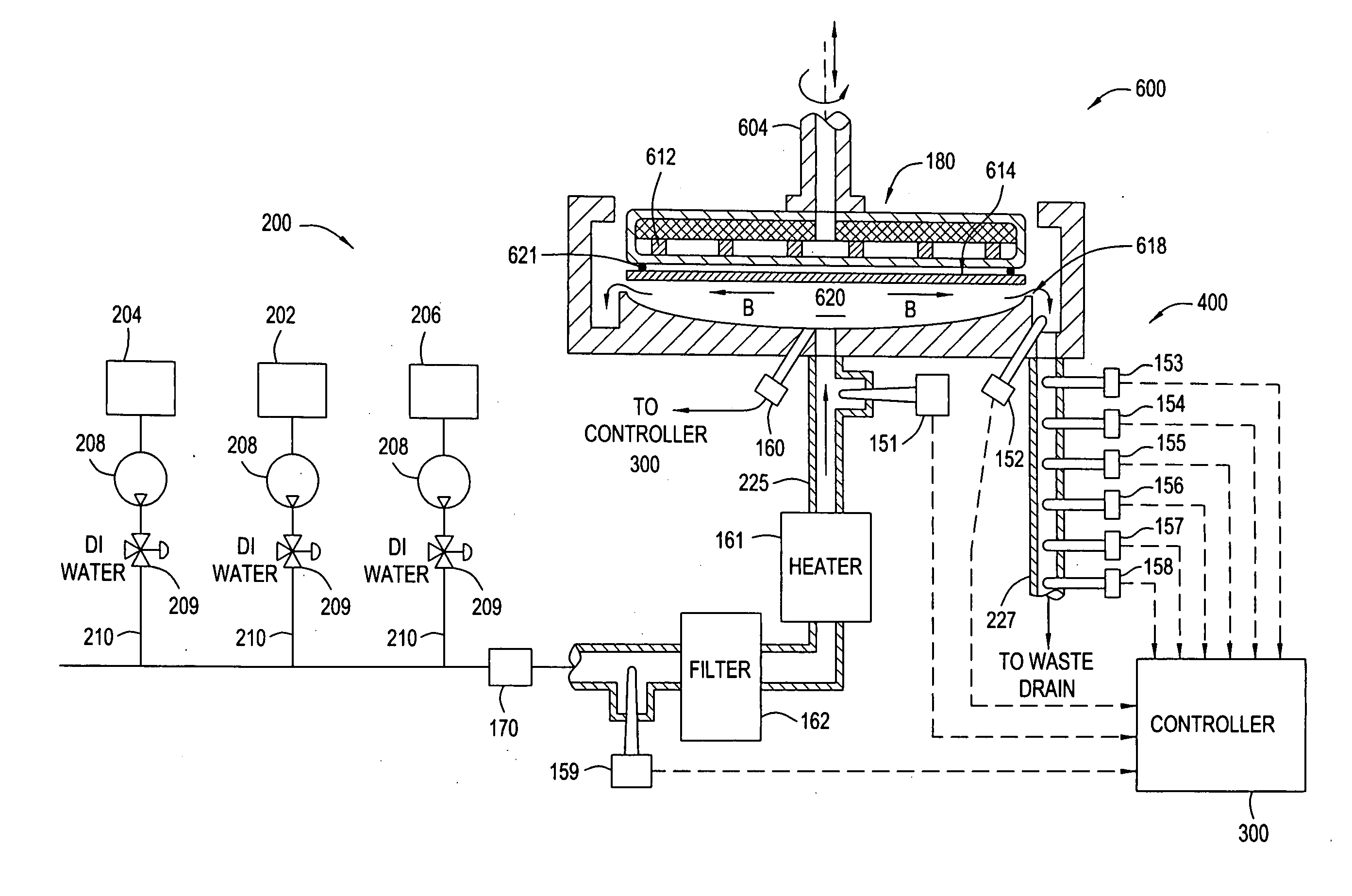
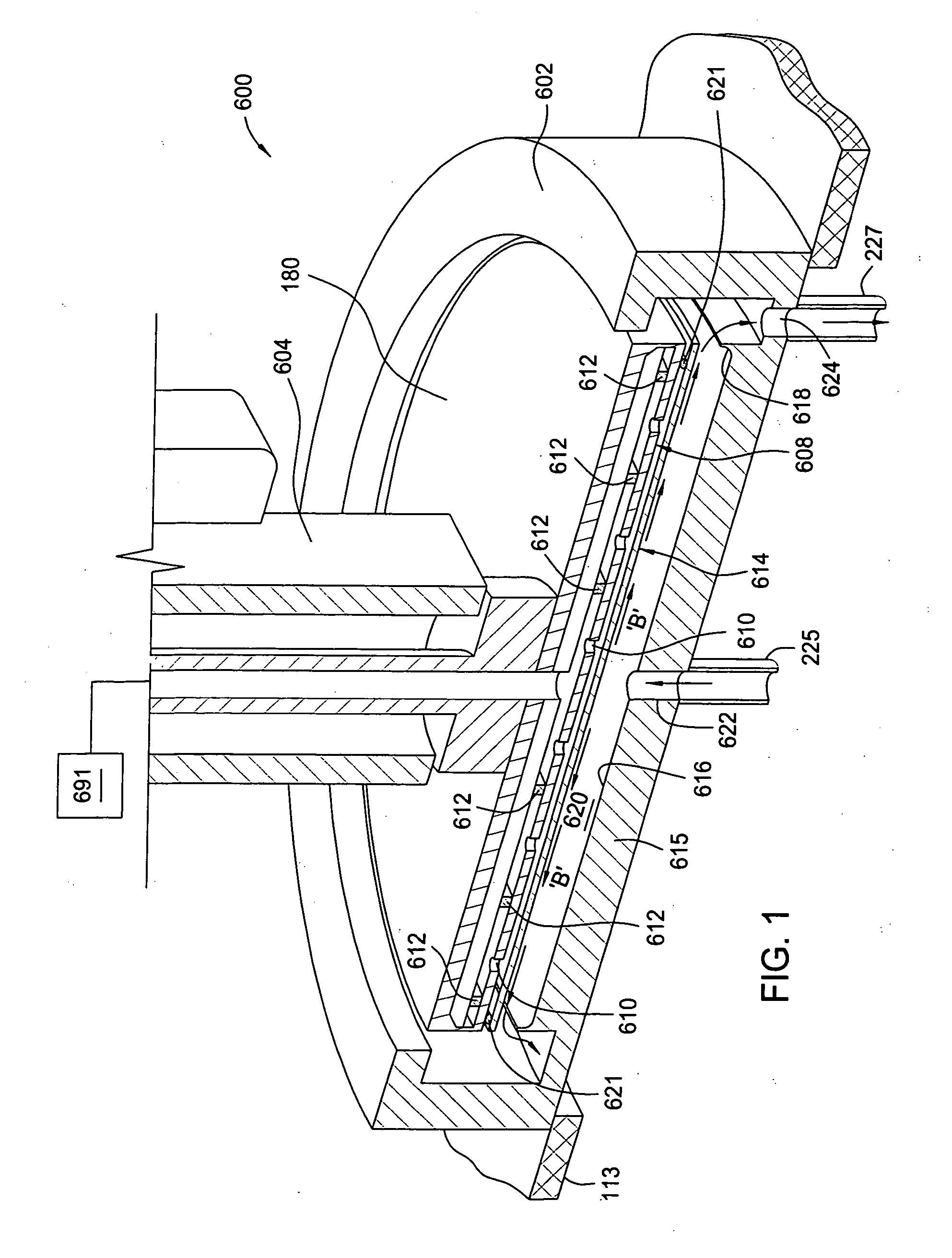
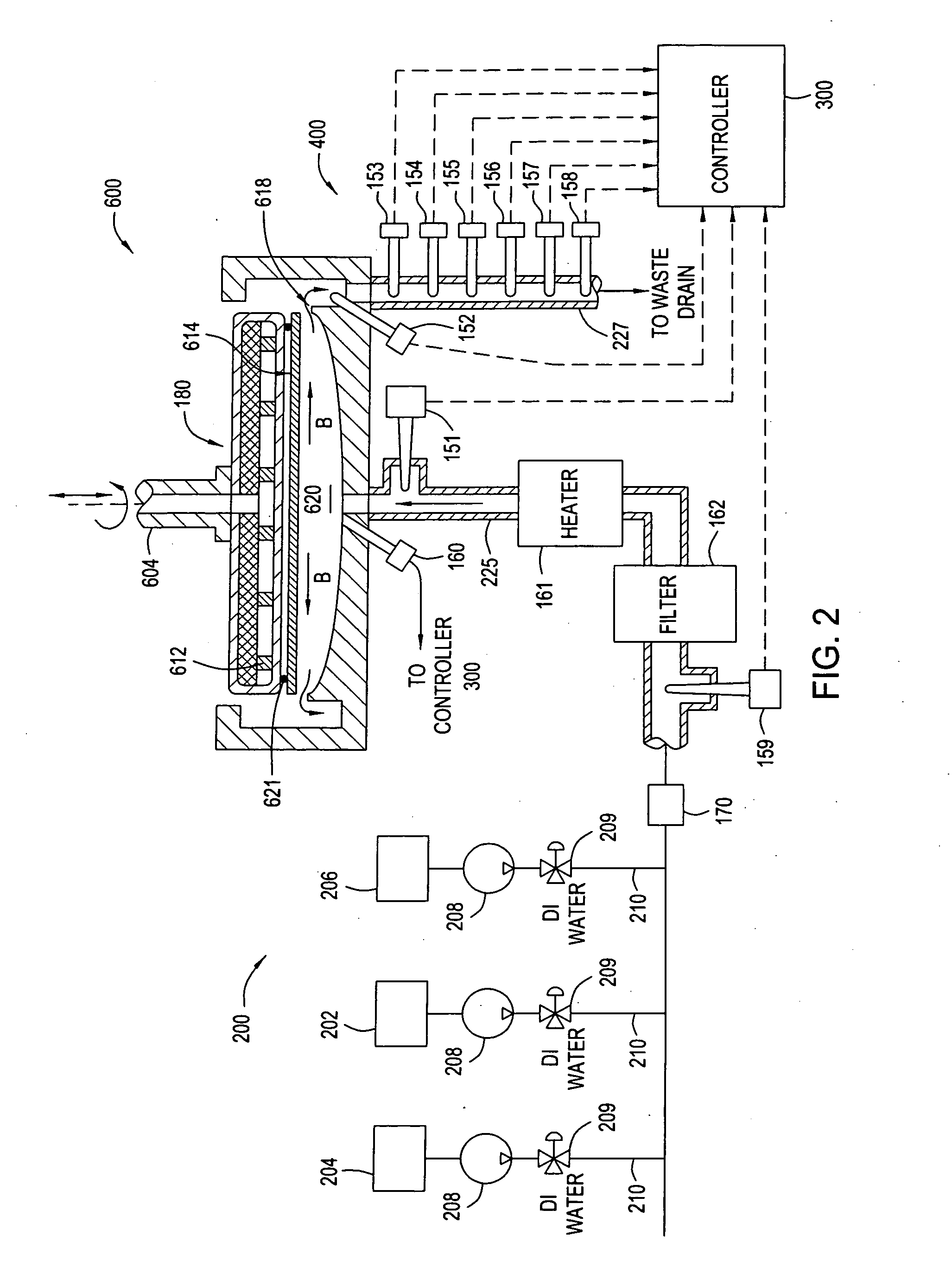
[0033] Embodiments of the invention generally provide an integrated electroless processing chamber that utilizes various process monitoring techniques to monitor and control the various electroless process steps, electroless chamber and supporting components. The electroless processing chamber can be a stand alone chamber or be integrated into a processing platform containing many pre- and post-electroless process chamber components. The term electroless process (or electroless deposition process) is meant to generally cover all process steps done to deposit an electroless deposited film onto a substrate including, for example, one or more of the pre-clean process steps (substrate preparation steps), the electroless activation process steps, the electroless deposition steps, and the post deposition cleaning steps. An exemplary electroless deposition processes is described in U.S. patent application Ser. No. 60 / 512,334 [AMAT 8660], entitled “Self-activating Electroless Deposition Pro...
PUM
| Property | Measurement | Unit |
|---|---|---|
| Time | aaaaa | aaaaa |
| Time | aaaaa | aaaaa |
| Time | aaaaa | aaaaa |
Abstract
Description
Claims
Application Information