Method of electrically connecting a microelectronic component

Inactive Publication Date: 2005-04-21
TESSERA INC
View PDF36 Cites 11 Cited by
  • Summary
  • Abstract
  • Description
  • Claims
  • Application Information

AI Technical Summary

Benefits of technology

[0015] One embodiment of the present invention provides a method of fabricating an interconnection component for a microelectronic device comprises providing a support structure, typically comprised of a flexible but substantially inextensible substrate, having a first and a second surface, where a conductive sheet is coupled to the first surface of the support structure. The conductive sheet is then selectively removed, typically using an etching process, thereby producing a highly planar, cost effective plurality of substantially rigid posts each of which eventually become the interconnections between the microelectronic device and a supporting substrate. The etching process generally first includes applying a photoresist layer to the conductive sheet and exposing portions of the photoresist layer to form etch resistant portions and remainder portions. The remainder portions may then be removed and the conductive sheet may be etched around the etch resistant portions. [00161 A compliant layer may then be provided on the second surface of the support structure and a microelectronic d

Problems solved by technology

Because the speed with which a microelectronic assembly can operate is inversely related to its size, this presents a serious drawback.
They generally do not allow use with chips having contacts disposed in an area array.
However, flip-chip assemblies suffer from significant problems when encountering thermal stress.
Changes in the relative sizes of the device and the supporting substrate due to thermal expansion and contraction in service create substantial stresses in these rigid bonds, which in turn can lead to fatigue failure of the bonds.
Moreover, it is difficult to test the chip before attaching it to the substrate, and hence difficult to maintain the required outgoing quality level in the finished assembly, particularly where the assembly includes numerous chips.
As the number of interconnections per microelectronic device increases, the issue of interconnection planarity continues to grow as well.
If the interconnections are not planar with respect to each other, it is likely that many of the interconnections will not electrically contact their juxtaposed contact pads on a supporting substrat

Method used


Image

  • Method of electrically connecting a microelectronic component
  • Method of electrically connecting a microelectronic component
  • Method of electrically connecting a microelectronic component

Examples


Example

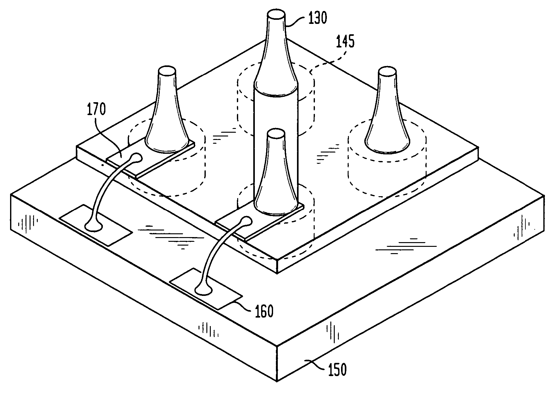
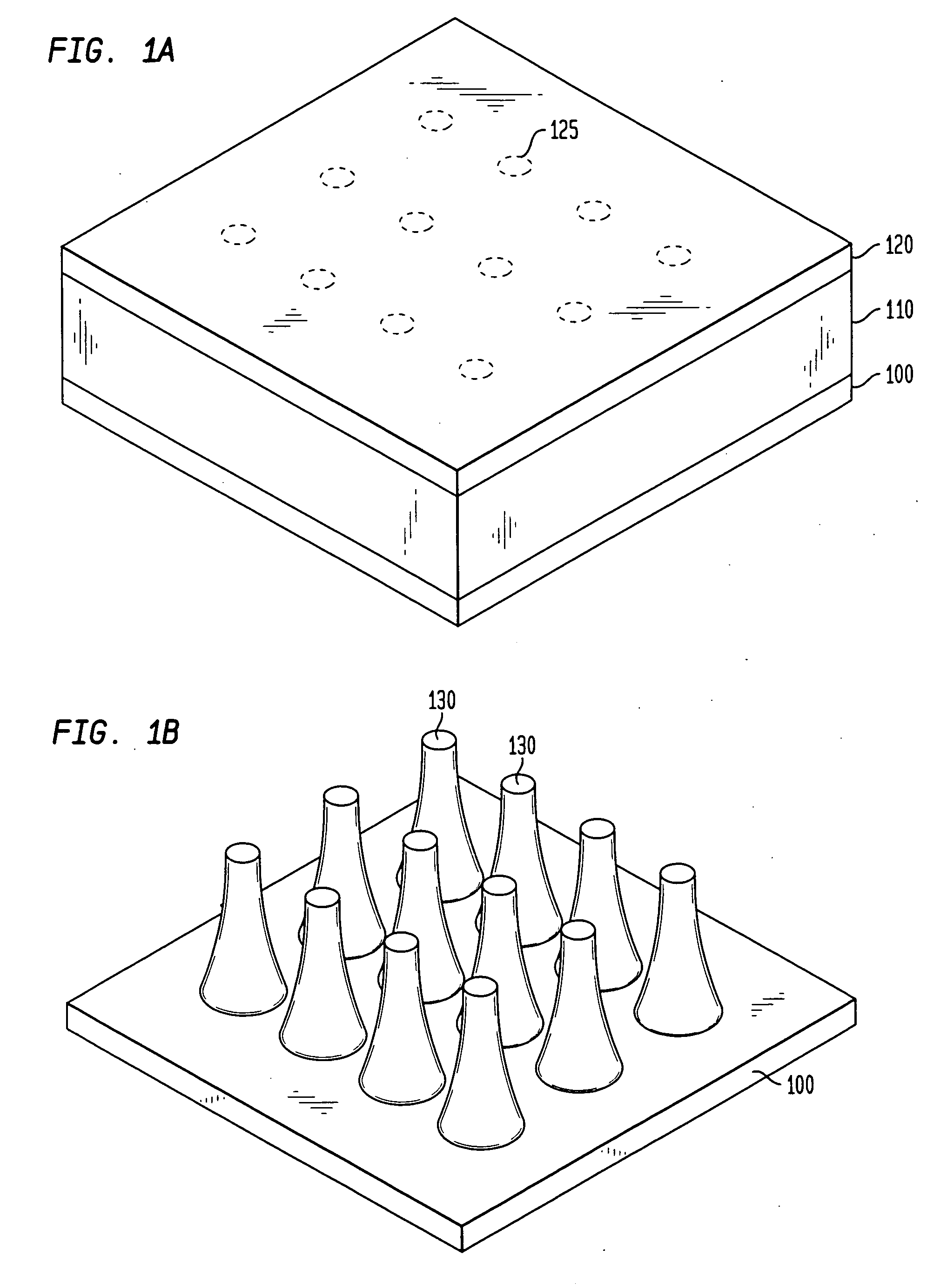
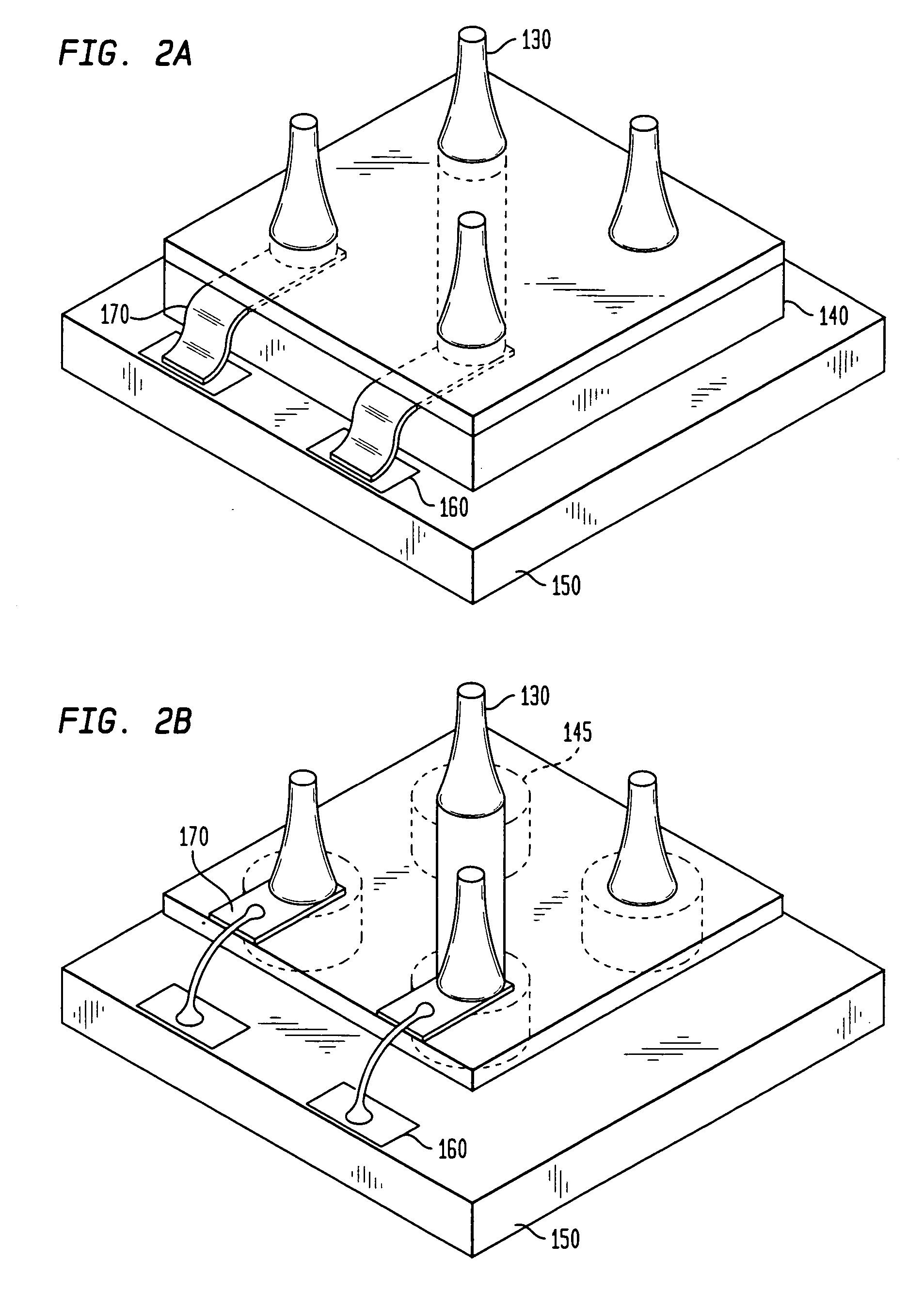
[0025] Referring to FIGS. 1A and 1B, a top surface of a support structure 100 is coupled to a conductive sheet 110. In the preferred embodiment of the invention, the support structure is a flexible, but substantially inextensible, film preferably formed from a polymeric material, such as Kapton™, of an approximate thickness between 25 microns and 75 microns and is laminated to the second surface of the conductive sheet. However, the support structure could be comprised of many other suitable materials and may further be semi-flexible or substantially rigid. The conductive sheet 110 is preferably comprised of a conductive metal, such as copper, copper alloys or phosphor bronze, among other materials. Portions of the conductive sheet are selectively removed by any suitable means to create a plurality of subtractively created, substantially rigid posts 130, as shown in FIG. 1B.

[0026] In the preferred embodiment, portions of the conductive sheet are removed by first providing a photore...


PUM

PropertyMeasurementUnit
Electrical conductivityaaaaaaaaaa
Electrical resistanceaaaaaaaaaa
Flexibilityaaaaaaaaaa

Abstract

A method of electrically connecting a microelectronic component having a first surface bearing a plurality of contacts. The method including the steps of forming a subassembly by juxtaposing a connection component having a support structure and a plurality of elongated posts extending substantially parallel to one another from a first surface of the support structure with the microelectronic component so that the support structure overlies the surface of the component with the posts extending away from the component and electrically connecting the posts to the contacts of the microelectronic component.

Description

CROSS-REFERENCE TO RELATED APPLICATIONS [0001] This application is a divisional of application Ser. No. 09 / 707,452 filed Nov. 7, 2000, which application is a divisional of co-pending U.S. patent application Ser. No. 08 / 885,238, filed on Jun. 30, 1997, which issued as U.S. Pat. No. 6,177,636 on Jan. 23, 2001 and which is a continuation of U.S. patent application Ser. No. 08 / 366,236 filed on Dec. 29, 1994, the disclosures of which are hereby incorporated herein by reference.FIELD OF THE INVENTION [0002] The present invention relates, generally, to interconnecting microelectronic devices and supporting substrates, and more particularly relates to an apparatus and a method of interconnecting microelectronic devices to supporting substrates using subtractively created members. BACKGROUND OF THE INVENTION [0003] Complex microelectronic devices such as modem semiconductor chips require many hundreds of input and output connections to other electronic components. These device connections ar...

Claims


Application Information

Patent Timeline
IPC IPC(8): H01L23/48H01L23/498
CPCH01L23/49811Y10T29/49126H01L24/72H01L2224/11003H01L2224/13099H01L2924/01013H01L2924/01015H01L2924/01027H01L2924/01029H01L2924/01046H01L2924/01078H01L2924/01079H01L2924/01082H01L2924/3025H01L2924/01005H01L2924/01006H01L2924/01033H01L2924/01047H01L2924/01076H01L2924/014H01L2924/00013H01L23/49816H01L24/13H01L24/11H01L2224/29099H01L2924/00H01L2224/11H01L2224/13H01L2924/12042H01L2924/351
Inventor FJELSTAD, JOSEPH C.
Owner TESSERA INC
Why Eureka
Try Eureka