Non-contact cool-down station for wafers

a technology of cool-down station and wafer, which is applied in the direction of domestic cooling apparatus, furniture, lighting and heating apparatus, etc., can solve the problems of damage to the cassette, inability to transport the wafer from the process chamber immediately,

Inactive Publication Date: 2005-05-05
ASM IP HLDG BV
View PDF40 Cites 19 Cited by
  • Summary
  • Abstract
  • Description
  • Claims
  • Application Information

AI Technical Summary

Problems solved by technology

Because of the high temperature CVD processing, transport of the wafer from the process chamber immediately to, e.g., a wafer cassette is not possible due to the temperature of the wafer exceeding the limits of heat resistance of the materials commonly used in the cassettes.
At these temperatures, the cassettes may be damaged and the structural integrity of the cassette may be undermined.
While cassettes are available that can handle wafers as hot as 170° C., they are relatively expensive.
Similarly, transfer of the wafers to a loadlock chamber immediately after high temperature processing is not possible because the temperature of a just-processed wafer may exceed the limits of the heat resistance of materials typically used to support the wafers in a loadlock.
As such, the structural integrity of the wafer support devices in the loadlock chamber may be undermined and the loadlock may be damaged.
Cooling the wafer on the susceptor is not cost-effective, however, because the process chamber is then unavailable for processing another wafer, thereby reducing the system wafer throughput.
This approach is particularly unattractive because it is then necessary to incur the delay and cost of reheating the wafer support structure or the chamber generally (in the case of hot wall chambers).
Removing a wafer while it is hot and cooling it on the wafer handling device is better, but also not cost effective because the delay in loading the next wafer slated for processing also compromises throughput, or requires additional wafer handling equipment and room for accommodating the same.
Such impediments increase the per-wafer cost, making these approaches financially unattractive to end users.
This approach to cooling wafers also has drawbacks, however, as the relatively hard pins can damage and leave scratches on the backside, or bottom surface, of the wafers by the force of the wafers being placed upon the pins.
In addition, contraction of a wafer while it cools on the pins can further scratch the wafer.

Method used


Image

  • Non-contact cool-down station for wafers
  • Non-contact cool-down station for wafers
  • Non-contact cool-down station for wafers

Examples


Embodiment Construction

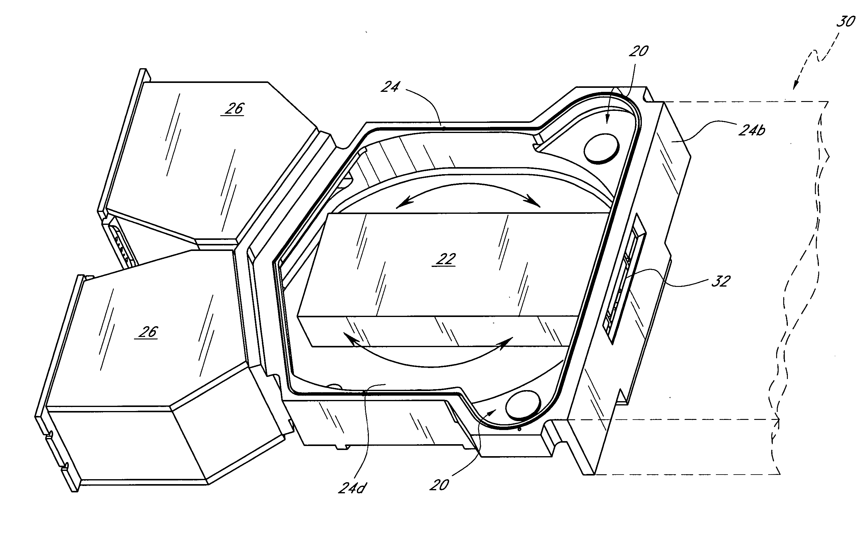
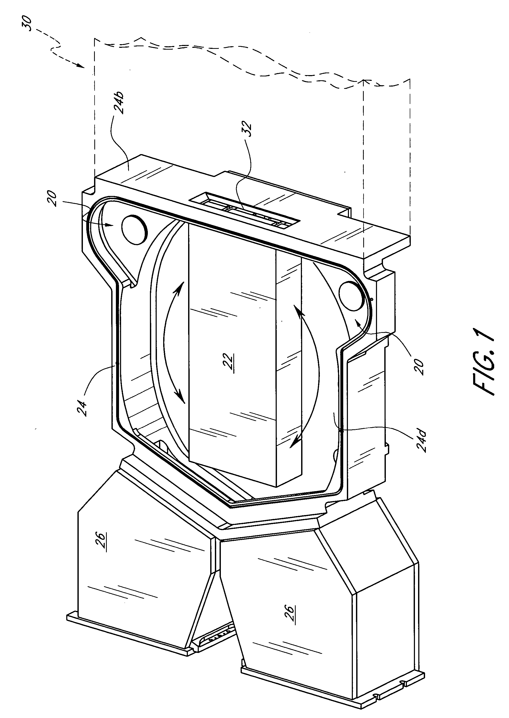
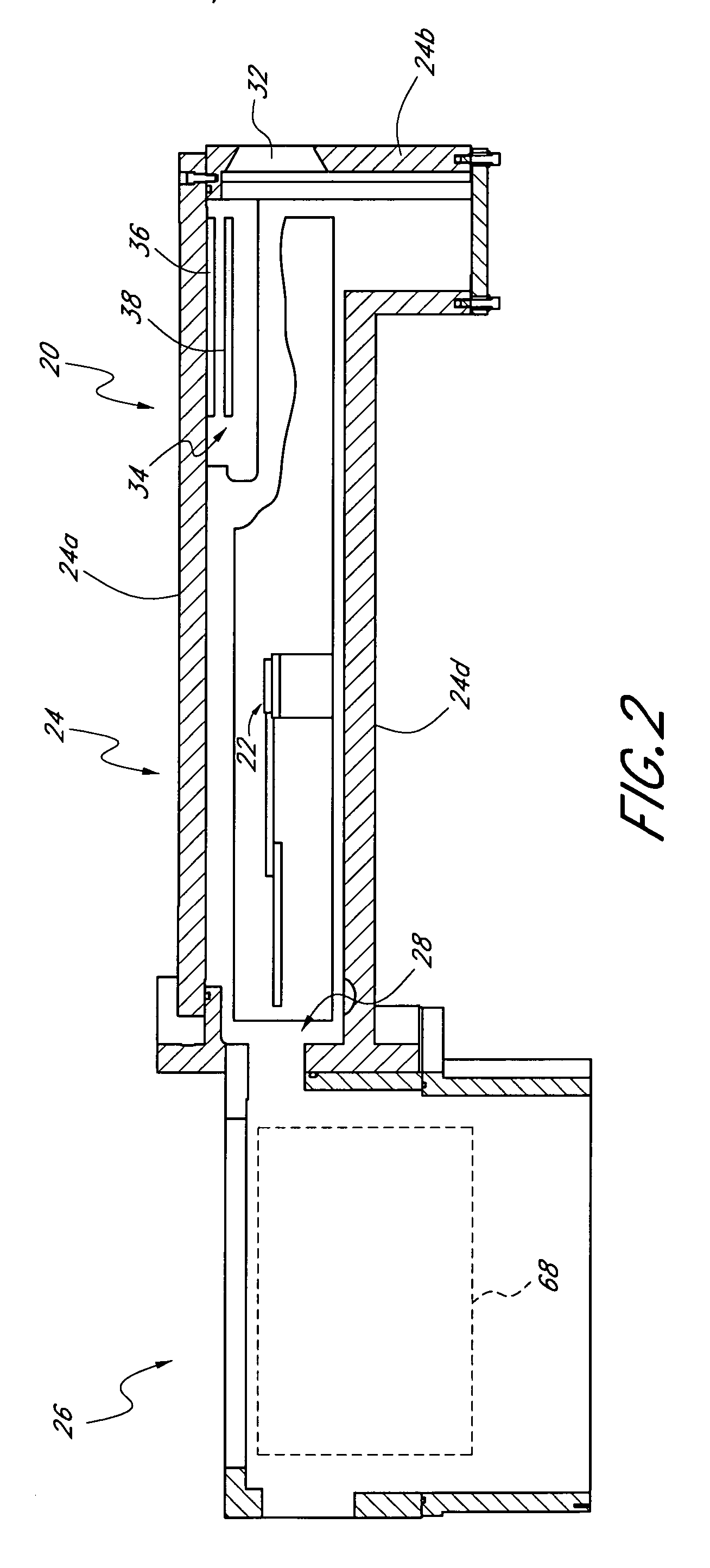
[0019] In the illustrated embodiments, a wafer station is provided in which a semiconductor wafer or substrate is held suspended by gas flowing across a major surface of the substrate in accordance with Bernoulli's principle. By this flow of gas, the substrate can be suspended without a horizontal surface of the substrate contacting another surface for vertical support. Advantageously, the wafer station can be used as a cooling station to cool substrates after undergoing semiconductor processing. In such an arrangement, the gas flowing across the major surface can be a cooling gas that cools the substrate as it flows across the major surface. In other arrangements, the wafer station can be used as a staging area to temporarily hold a wafer before the wafer is transported elsewhere.

[0020] In suspending the substrate by taking advantage of the Bernoulli principle, the wafer station operates in a manner similar to a class of semiconductor pick-up devices called Bernoulli wands. Bernou...


PUM

PropertyMeasurementUnit
temperatureaaaaaaaaaa

Abstract

A stationary cooling station for cooling wafers after the wafers have been subjected to semiconductor processing supports the wafer by flowing gas in accordance with the Bernoulli principle. An upper wall of the cooling station contains a plurality of gas outlets that direct gas to flow over the top surface of the wafer. In this way, a low-pressure region is created over the wafer and the wafer is suspended within the cooling station, without directly contacting any surface for support. In addition to providing lift for the wafer, the gas is a thermally conductive gas that can cool the wafer by conducting heat away from it.

Description

FIELD OF THE INVENTION [0001] This invention relates generally to semiconductor fabrication and, more particularly, to an apparatus and a method for cooling a substrate at a cool-down station. BACKGROUND OF THE INVENTION [0002] Semiconductor wafers or other such substrates are subjected to very high processing temperatures. For example, in high temperature epitaxial chemical vapor deposition (CVD), the temperatures can approach 1200° C., while low temperature epitaxy is conducted between about 400° C. and 900° C. In a typical cycle, using one or more robotic wafer handlers, a wafer is transferred from a room temperature cassette either directly, or via one or more loadlock and transfer chambers, into a processing or reaction chamber where the wafer is subjected to high temperature processing. The wafer is then transferred using one or more wafer handlers from the high temperature processing chamber back to the same cassette or a separate cassette for processed wafers, either directl...

Claims


Application Information

Patent Timeline
Patent Type & Authority Applications(United States)
IPC IPC(8): H01L21/00
CPCH01L21/67196H01L21/67109
Inventor AGGARWAL, RAVINDERHARO, BOB
Owner ASM IP HLDG BV
Why Eureka
Try Eureka