Impedance circuit, and filter circuit, amplifier circuit, semiconductor integrated circuit, electronic component, and wireless communications device using the same

a filter circuit and filter circuit technology, applied in the direction of multiple-port networks, electrical devices, waveguide-type devices, etc., can solve the problems of reducing the number of components and the occupied area, and unable to achieve a circuit capable of attaining a satisfactory characteristic across all the usable bands, so as to reduce the size of the wireless communication device

Inactive Publication Date: 2005-05-05
SEIKO EPSON CORP
View PDF8 Cites 72 Cited by
  • Summary
  • Abstract
  • Description
  • Claims
  • Application Information

AI Technical Summary

Benefits of technology

[0054] According to the seventeenth aspect, an amplifier circuit, provided with a matching circuit capable of performing processing in response to more than one frequency band, can be achieved by using fewer components. Hence, by using this semiconductor integrated circuit, it is possible to reduce the size of a wireless communications device using an amplifier circuit.

Problems solved by technology

This is because it is practically difficult to achieve a circuit capable of attaining a satisfactory characteristic across all the usable bands, as respective circuits forming the RF portion.
Even when a circuit is configured to attain a homogeneous characteristic across all the bands, the performance of such a circuit markedly deteriorates compared with a case where a circuit is formed separately for each usable frequency band.
However, in a case where a signal path forming the RF portion is provided separately for each frequency band to be used as described above, the number of components and an occupied area are increased, which makes it difficult to reduce the cost and the size of the circuits.
In the case of a filter circuit, however, when a frequency band allowed to pass is changed by adjusting the resonance frequency as described above, there arises a need to use a low-Q element, such as a varactor diode, in the resonant circuit, which poses a problem in that the filter characteristic is deteriorated.
In particular, in terms of the area occupied by the circuits, the input and output matching circuits occupy a larger area than the active element portion, which poses a problem in that this configuration is less effective in achieving a fundamental reduction of the circuit size.
In addition, when the matching circuit is a matching circuit covering a broad band including usable frequencies and the circuit to be matched is an amplifier, a signal in a frequency band other than the desired frequency band is also amplified, which makes this configuration disadvantageous in terms of efficiency of the amplifier.

Method used


Image

  • Impedance circuit, and filter circuit, amplifier circuit, semiconductor integrated circuit, electronic component, and wireless communications device using the same
  • Impedance circuit, and filter circuit, amplifier circuit, semiconductor integrated circuit, electronic component, and wireless communications device using the same
  • Impedance circuit, and filter circuit, amplifier circuit, semiconductor integrated circuit, electronic component, and wireless communications device using the same

Examples


first embodiment

[0079] First, a first embodiment will be described.

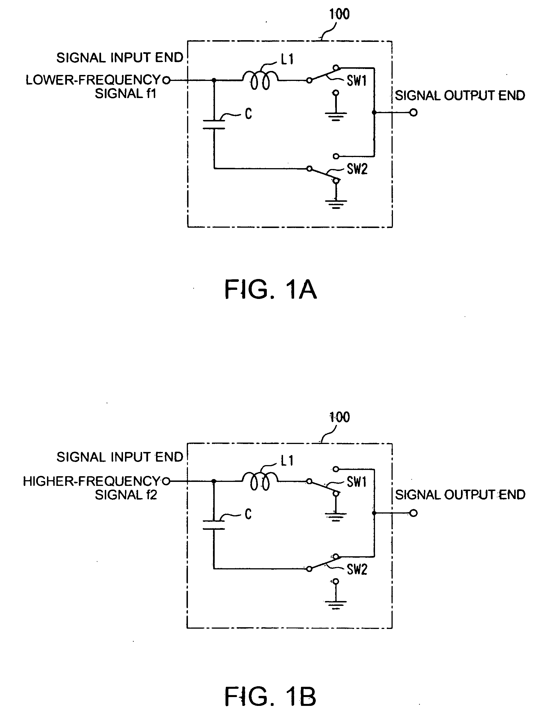
[0080]FIG. 1 is a circuit diagram showing one example of a filter circuit 100 using an impedance circuit of the invention.

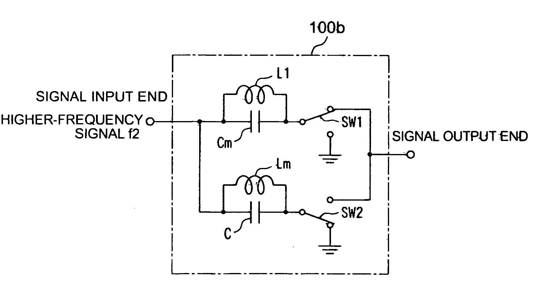
[0081] The filter circuit 100 according to the first embodiment comprises, as is shown in FIG. 1(a), an inductor L1 and a capacitor C which are lumped elements, and switch circuits SW1 and SW2. The inductor L1 forms a first impedance element and the capacitor C forms a second impedance element, while the switch circuits SW1 and SW2 form a first switch and a second switch respectively.

[0082] One end of the inductor L1 is connected to one end of the capacitor C to form a signal input end. Also, the other end of the inductor L1 is connected so the switch circuit, SW1, and the other end of the capacitor C is connected to the switch circuit SW2.

[0083] The switch circuit SW1 selectively connects the other end of the inductor L1 to either ground or a signal output end. Likewise, the switch circuit SW2 selectively con...

second embodiment

[0102] the invention will now be described.

[0103] A filter circuit 200 according to the second embodiment is, as is shown in FIG. 4, a filter circuit formed by using an inductor L2 which is a distributed element, instead of the inductor L1 which is a lumped element in the first embodiment shown in FIG. 1.

[0104] In this case, too, when a lower-frequency signal f1 is to be processed, as is shown in FIG. 4(a), the inductor L2 is connected to the signal output end and the capacitor C is connected to ground by manipulating the switch circuits SW1 and SW2 to form a low-pass filter circuit. In contrast, when a higher-frequency signal f2 is to be processed, as is shown in FIG. 4(b), the capacitor C is connected to the signal output end and the inductor L2 is connected to ground to form a high-pass filter circuit.

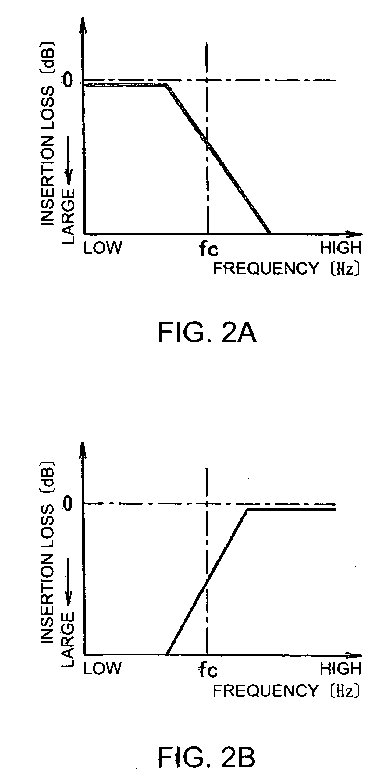
[0105]FIG. 5 shows a simulation result of a filter output from the filter circuit 200 shown in FIG. 4 when signal frequencies were varied, using a signal in the 2.4 GHz band as th...

third embodiment

[0110] the invention will now be described.

[0111]FIG. 6 shows the configuration of a filter circuit 300 according to the third embodiment, and as is shown in FIG. 6, the circuit 300 comprises a first filter portion 12, and a second filter portion 14 that uses an output of the first filter portion 12 as an input.

[0112] Each of the first filter portion 12 and the second filter portion 14 comprises the filter circuit 100 in the first embodiment, so that the first filter portion 12 and the second filter portion 14 are configured to have equal filter characteristics.

[0113] By connecting the first filter portion 12 and the second filter portion 14 having equal characteristics, that is, by connecting the filter circuits 100 in more than one stage, more rapid filter processing is enabled.

[0114] This embodiment described a case where the filter circuits are connected in two stages. However, when there is a need to secure a further sharper filter characteristic, the filter circuits are con...


PUM


Abstract

A filter circuit is provided wherein one end of an inductor is connected to one end of a capacitor to form a signal input end. The other end of the inductor is connected to a first switch circuit, and the other end of the capacitor is connected to a second switch circuit. When a lower-frequency signal in a 2.4 GHz band is to be inputted, a low-pass filter circuit is formed by connecting the other end of the inductor to a signal output end and the other end of the capacitor to ground, and when a higher-frequency signal in a 5 GHz band is to be inputted, a high-pass filter circuit is formed by connecting the other end of the inductor to ground and the other end of the capacitor to the signal output end, by manipulating the first and second switch circuits.

Description

RELATED APPLICATIONS [0001] This application claims priority to Japanese Patent Application Nos. 2003-331598 filed Sep. 24, 2003, 2003-331599 filed Sep. 24, 2003, and 2004-133684 filed Apr. 28, 2004 which are hereby expressly incorporated by reference herein in their entirety. BACKGROUND [0002] 1. Technical Field [0003] The present invention relates to a filter circuit used in a wireless communications device or the like and an impedance circuit, such as a matching circuit, and more particularly to an impedance circuit capable of operating in response to more than one frequency band, and a filter circuit, an amplifier circuit, a semiconductor integrated circuit, an electronic component, and a wireless communications device using such an impedance circuit. [0004] 2. Background Art [0005] A system that uses switching over more than one frequency band has recently become known in a communications system. For example, in the wireless LAN method, the system switches from a 2.4 GHz band t...

Claims


Application Information

Patent Timeline
Patent Type & Authority Applications(United States)
IPC IPC(8): H03H7/01H03H7/075H03H7/12H03H7/38H03H7/46
CPCH03H7/46H03H7/383H03H7/38H03H7/12
Inventor WATANABE, TORUINOGUCHI, MAKOTO
Owner SEIKO EPSON CORP
Why Eureka
Try Eureka