Zero insertion force high frequency connector

a high-frequency connector, zero-injection-force technology, applied in the direction of coupling contact members, fixed connections, coupling device connections, etc., can solve the problems of bending one or more pins, each type of pins suffers from common problems, and the backplane typically provides little functionality, etc., to achieve easy replacement and serviceability. , the effect of easy replacemen

Active Publication Date: 2005-05-05
CARLISLE INTERCONNECT TECH
View PDF44 Cites 14 Cited by
  • Summary
  • Abstract
  • Description
  • Claims
  • Application Information

AI Technical Summary

Benefits of technology

[0020] The present invention addresses the above drawbacks and provides the benefits of an elastomeric connector, while providing high frequency data and / or communications connections between two electrical circuit boards or other components. To this end, and in accordance with principles of the present invention, a connector assembly includes a circuit board or component having at least one shielded land area and a signal array including at least one shielded conductor having at least one central conductive core and a conductive outer structure. A connector of insulating material with two faces and conductive elements extending from face to face is coupled between the circuit board / component and the shielded conductor of the array to pass a high speed data and / or communications signal from the shielded conductor to the land areas of the circuit board / component.
[0021] The connector assembly of the invention maintains the geometric arrangement of the shielded conductor through the connector to the land areas. The connector assembly is also easily replaced requiring no soldering and is, therefore, easily and readily serviceable.

Problems solved by technology

A backplane typically provides little functionality other than electrically interconnecting the circuit boards within the circuit packs.
Irrespective of whether one of these connectors is a through hole or surface mount type, each type suffers from common problems once attached to a circuit board.
Any deviation in alignment when plugging one connector into another can result in the bending of one or more of these pins.
This generally causes either a failure of the product under production test, or worse, a failure of the product in the possession of a user or consumer.
This is can be a difficult process, and at the very least, is a time consuming one.
This subjects the board, as well other components adjacent to the connector, to a substantial amount of heat.
A heat gun in the hands of an inexperienced repair technician can result in the board being ruined, or the adjacent components being damaged.
Even when a heat gun is not used, replacement of a surface mount connector can take a considerable amount of time, and still requires a skilled technician.
Again, this makes removal difficult, increasing the chances for an unskilled technician to damage the board or surrounding components.
In some cases, with connectors having a large array of pins, it becomes impractical, if not impossible, to simultaneously re-flow the solder on every pin.
Another problem inherent in the afore described connectors is that the geometric arrangement and / or spacing between pins is not maintained through the connector to the surface of a respective circuit board.
Deviation in the geometric arrangement and / or spacing of between pins when used as a pair generally results in impedance variation with a change in frequency, thereby degrading the electrical performance of the connector and / or limiting the usable frequency range of the connector.
Such connectors provide no shielding, nor is consistent spacing possible.
However, signals between an LCD screen and a circuit board are low frequency digital signals not high frequency data / communications signals.
Therefore, such connectors have not been particularly suited to the transfer of high frequency signals, e.g., data and / or communications signals in a connector assembly between two circuit boards.

Method used


Image

  • Zero insertion force high frequency connector
  • Zero insertion force high frequency connector
  • Zero insertion force high frequency connector

Examples


Embodiment Construction

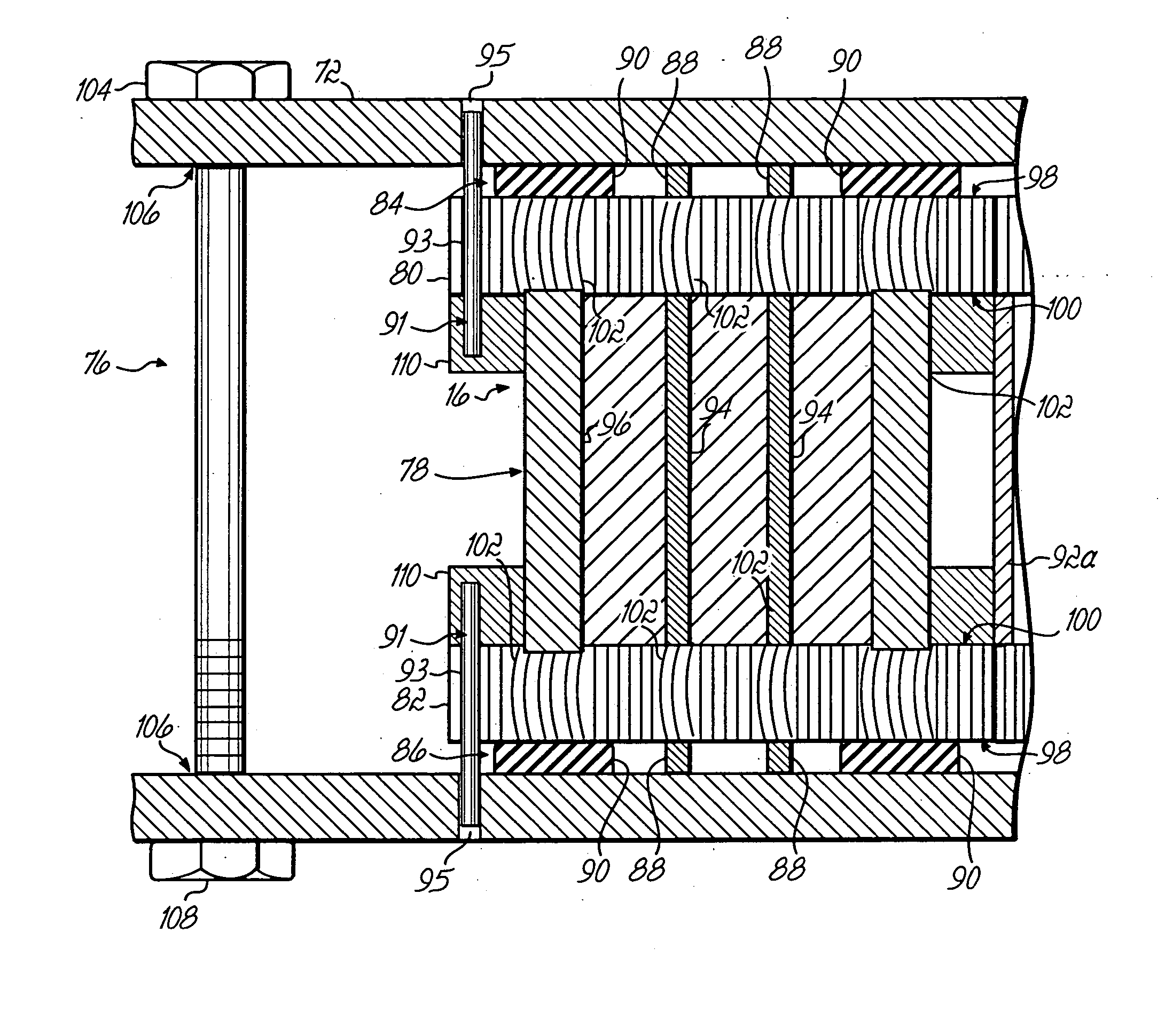
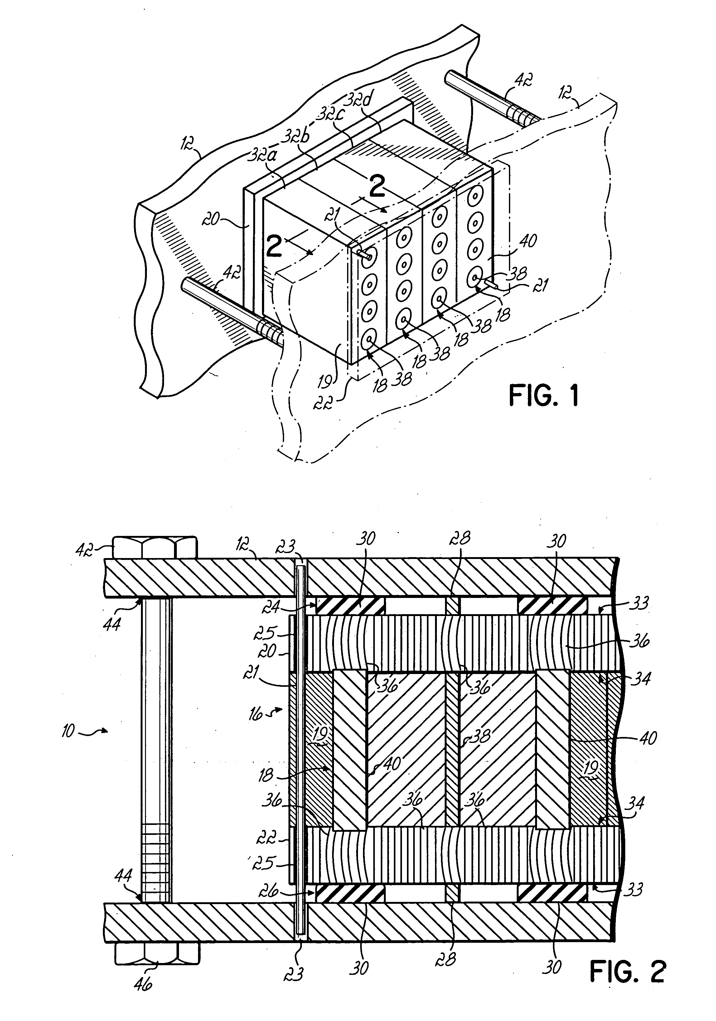
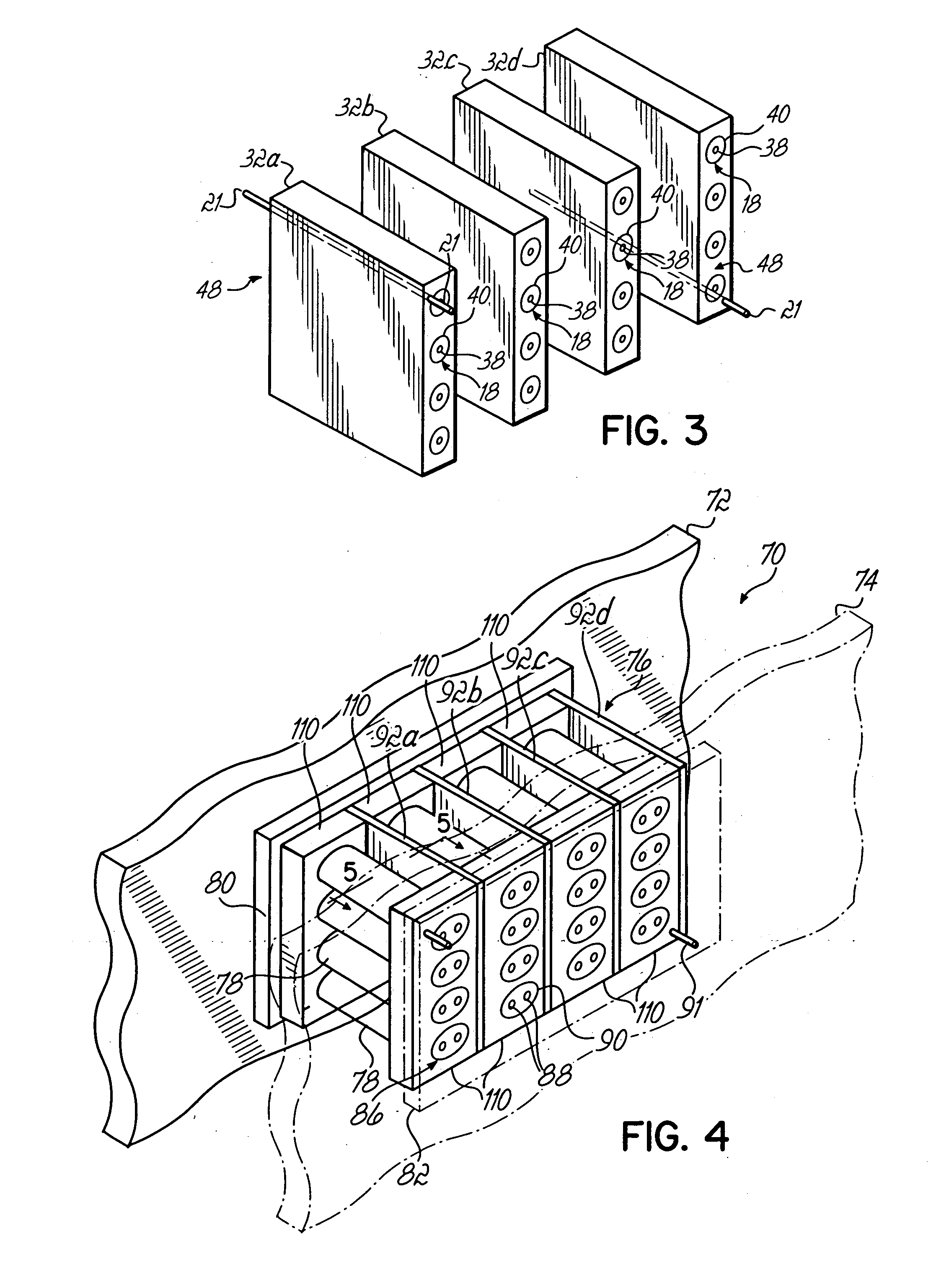
[0037] Referring to FIGS. 1 and 2, connector assembly 10 comprises two substantially parallel oriented components, such as circuit boards 12, 14 (circuit board 14 shown in phantom line), a signal array 16 including at least one shielded conductor 18, and compressible interface elements 20, 22 (compressible interface element 22 also shown in phantom line) coupled between each circuit board 12, 14 and shielded conductor 18. Circuit boards 12, 14 include corresponding shielded land areas 24, 26, only shielded land area 26 being shown in FIG. 1. Shielded conductor 18 has opposite ends and includes an axial conductive element 38 and an outer conductive element 40 surrounding the axial conductive element 38. Shielded land areas 24, 26 include a central conductive core area 28 and a conductive outer structure area 30. Land areas 24, 26 on circuit boards 12, 14 may be etched, deposited, or other placed using methods well known to those of skill in the art.

[0038] Although not shown for ease...


PUM


Abstract

A connector or connector assembly having a signal array having at least one shielded conductor having opposite ends and including an axial conductive element and an outer conductive element surrounding the axial conductive element and a compressible interface element positioned at least one of the opposite ends of the signal array, the interface element including a layer of insulating material having a plurality of conductive elements extending through the insulating material layer. When compressed between the signal array and a signal bearing component, the compressible interface element maintains the geometric arrangement of the axial conductive element and the outer conductive element to the signal bearing component. A connector assembly may include a circuit board including land areas arranged in a shielded configuration, and corresponding to the shielded land areas on the component and a second compressible interface element. The compressible interface element is coupled between the circuit board and the shielded conductor to pass a signal from the shielded conductor to the land area on the second circuit board.

Description

FIELD OF THE INVENTION [0001] This present invention relates generally to electrical connectors, such as those used to electrically couple two circuit boards together and particularly to improving the performance, construction and ease of use of such electrical connectors. BACKGROUND OF THE INVENTION [0002] The use of electronic products of all kinds has increased dramatically throughout society, which has led to a significant increase in the demand for improved components utilized within such products. One facet in the utilization of such electronic products involves the coupling of high frequency signals, e.g., data and / or communications signals, between various electronic circuit boards contained within such products. [0003] Some electronic products include a rack or frame into which multiple circuit packs are inserted. Generally, a frame includes a circuit board referred to as a “backplane”, while a circuit pack may include one or more circuit boards. A backplane generally inclu...

Claims


Application Information

Patent Timeline
Patent Type & Authority Applications(United States)
IPC IPC(8): H01R13/24
CPCH01R13/2414H01R12/714H01R12/52H01R12/7082H01R12/73H01R12/735H05K1/144H05K2201/0314H05K2201/042H05K2201/10378
Inventor TUTT, CHRISTOPHER ALAN
Owner CARLISLE INTERCONNECT TECH
Why Eureka
Try Eureka