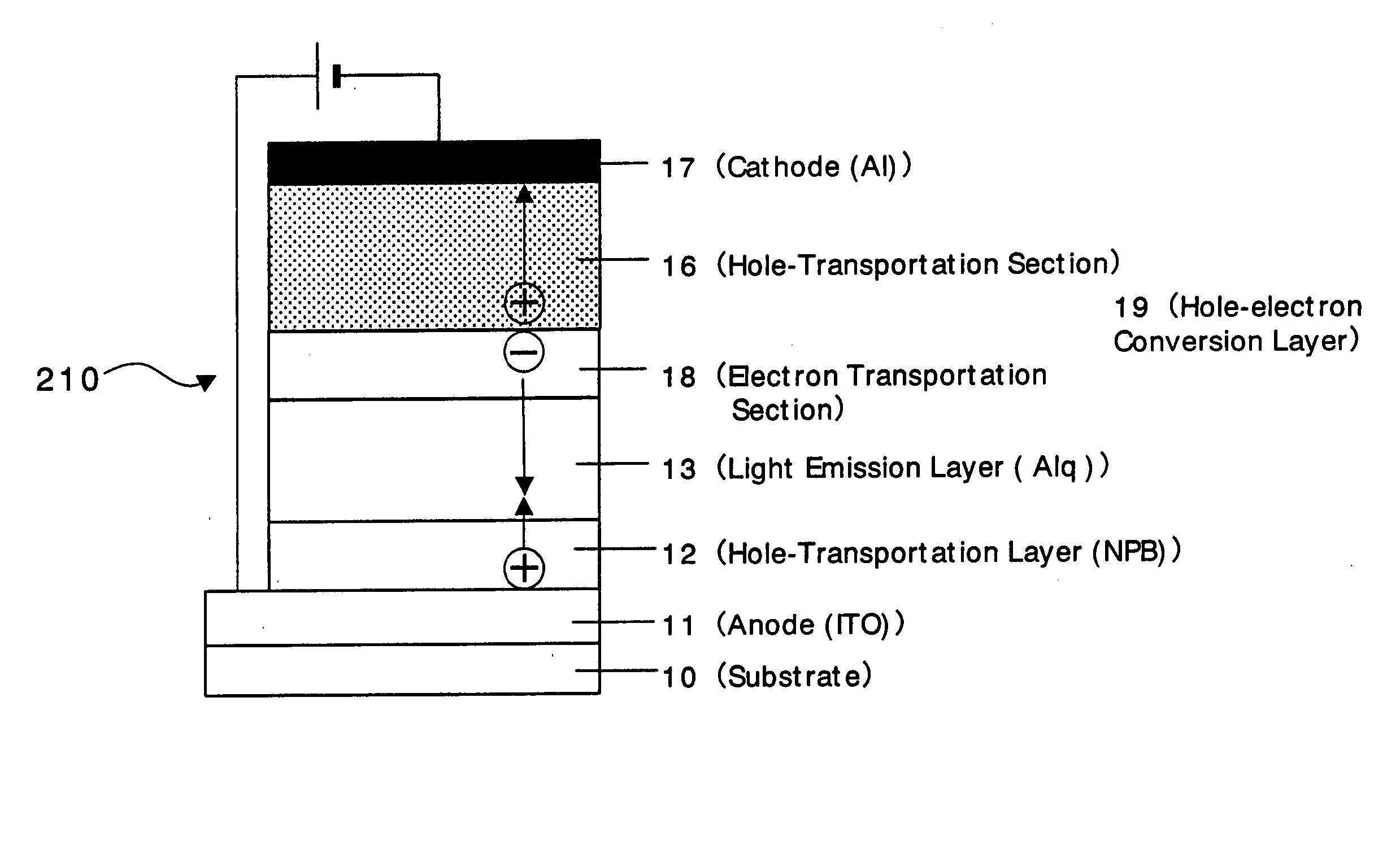
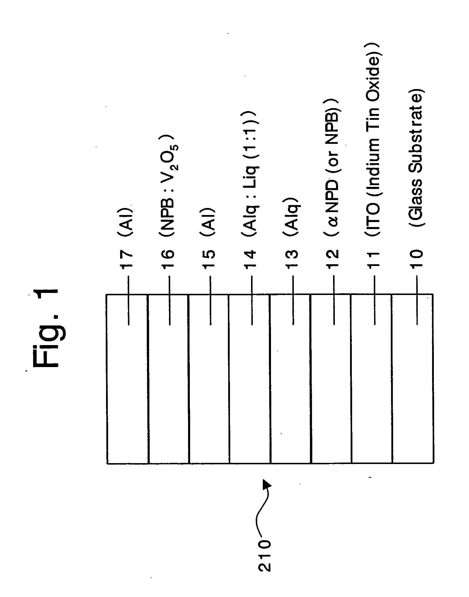
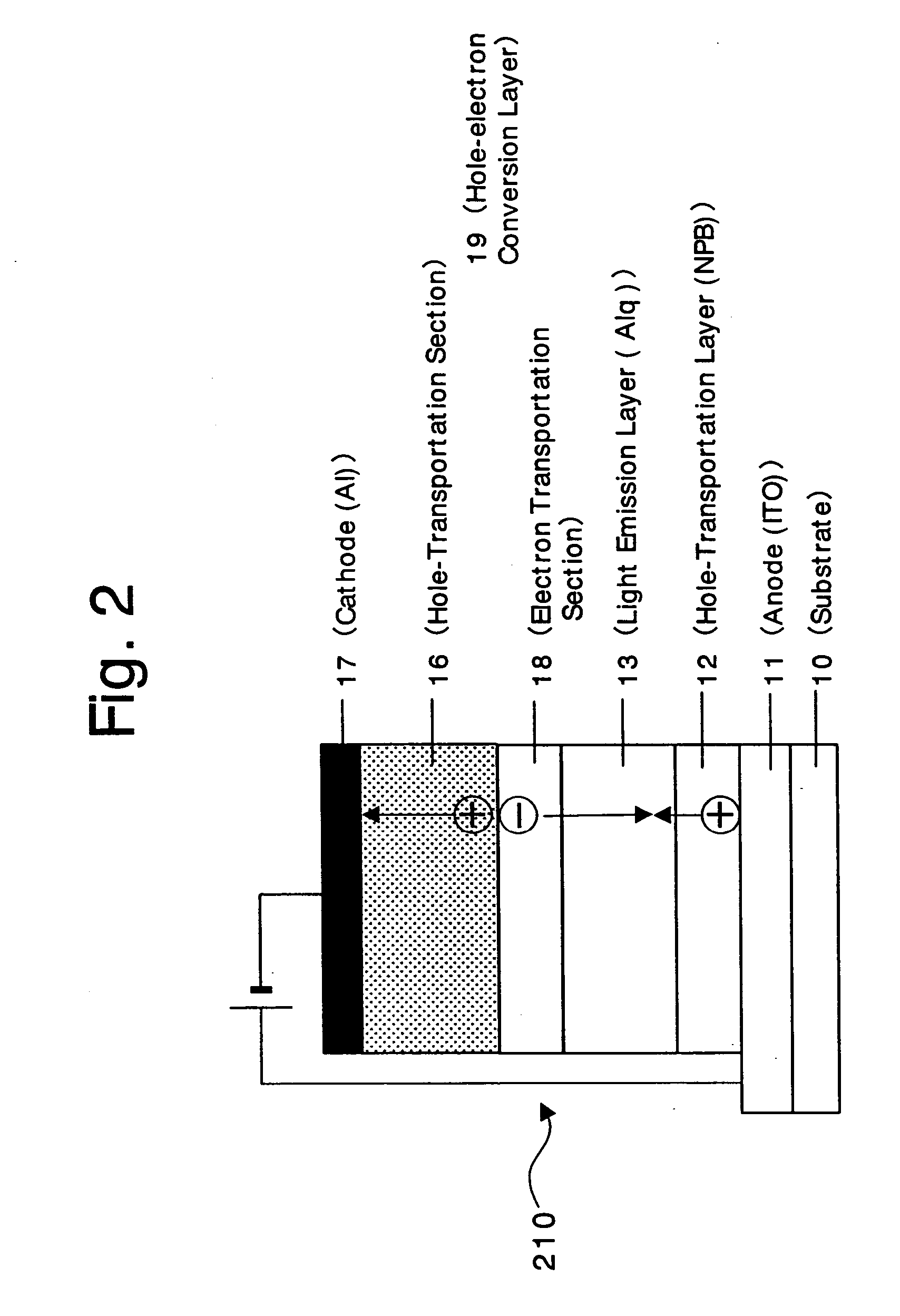
Organic devices, organic electroluminescent devices, organic solar cells, organic FET structures and production method of organic devices

a technology of electroluminescent devices and organic solar cells, which is applied in the direction of discharge tube luminescnet screens, sustainable manufacturing/processing, and final product manufacturing, etc., can solve the problems of difficult electron transfer, power conversion efficiency cannot be substantially improved or changed, and mpe devices showing good performance like those plotted in fig. 24 cannot be realized with eas

Active Publication Date: 2005-05-12
MITSUBISHI HEAVY IND LTD +1
View PDF20 Cites 328 Cited by
  • Summary
  • Abstract
  • Description
  • Claims
  • Application Information

AI Technical Summary

Benefits of technology

[0056] An organic field effect transistor structure can include the organic device.

Problems solved by technology

In this case, since the driving voltage is also increased to approximately (n+1) times, it was expected in theory that the power conversion efficiency cannot be substantially improved or changed.
The MPE devices showing good performances like ones plotted in FIG. 24 cannot be realized with ease.
2866 (1998), i.e., the radical anion molecules are produced through direct doping of electron donors (reducing dopants) such as alkaline metals, problems arise such as undesirable reactions occurring unintentionally between the electron donors (reducing agents) and the electron acceptors (oxidizing agents), between the electron-accepting organic compound and the oxidizing agents, and also between the electron-donating molecules (hole-transporting molecules) and the electron donors (reducing agents), to thereby make difficult the transfer of the electrons.

Method used


Image

  • Organic devices, organic electroluminescent devices, organic solar cells, organic FET structures and production method of organic devices
  • Organic devices, organic electroluminescent devices, organic solar cells, organic FET structures and production method of organic devices
  • Organic devices, organic electroluminescent devices, organic solar cells, organic FET structures and production method of organic devices

Examples


first embodiment

[0087] In the first embodiment of the present invention, a lithium complex of (8-quinolinolato) (hereinafter, referred to as “Liq”) represented by the following formula:

is used as an organic metal compound containing ions of low work function metals (for example, alkaline metals) having a work function of not more than 4.0 eV, typically alkaline metal ions, alkaline earth metal ions, rare earth metal ions and some transition metal ions, in the formation of the electron transportation section (thermal reduction reaction-generated layer).

[0088] Furthermore, an organic compound such as an aluminum complex of tris(8-quinolinolato) (hereinafter, referred to as “Alq”) represented by the following formula:

or bathocuproine (hereinafter, referred to as “BCP”) represented by the following formula:

is used as an organic electron-accepting (electron-transporting) compound. According to one suitable method for forming the electron transportation section according to the present inventio...

second embodiment

[0091] In the second embodiment of the present invention, as in the first embodiment described above, an organic metal complex containing alkaline metal ions such as Liq as an organic metal compound containing ions of low work function metals (for example, alkaline metals), an organic electron-accepting (-transporting) compound such as Alq and a thermally reducible metal such as aluminum can be used in the formation of the electron transportation section (thermal reduction reaction-generated layer). These three compounds can be simultaneously deposited and mixed (ternary co-deposition) to form the electron transportation section having the functions similar to those of the first embodiment. In this co-deposition process, when a deposition rate of the three compounds is suitably and precisely controlled, it becomes possible in the organic devices to obtain a layer having a high transparency and a good (low) resistivity comparable to that of the electron transportation layer having in...

third embodiment

[0092] In the third embodiment of the present invention, an organic metal complex containing rare earth metal ions such as an europium complex of tri(1,3-phenyl -1,3-propanedionato)mono(bathophenanthroline) (hereinafter, referred to as “Eu(DBM)3.BPEHEN”) represented by the following formula:

in which one of the ligands is a compound which shows the electron-accepting (-transporting) property by itself, for example, bathophenanthroline) (hereinafter, referred to as “BPEHEN”) represented by the following formula:

can be used in the formation of the electron transportation section (thermal reduction reaction-generated layer). The compound Eu(DBM)3.BPEHEN and a thermally reducible metal such as aluminum can be simultaneously deposited and mixed (binary co-deposition) to form the electron transportation section having the functions similar to those of the first and second embodiments. In this co-deposition process, when a deposition rate of the two compounds is suitably and precisely...


PUM

PropertyMeasurementUnit
work functionaaaaaaaaaa
ionization potentialaaaaaaaaaa
glass transition temperatureaaaaaaaaaa

Abstract

An organic device has a hole current-electron current conversion layer which comprises a laminate of an electron transportation section and a hole transportation section. The electron transportation section includes a charge transfer complex formed upon an oxidation-reduction reaction between a reduced low work function metal and an electron-accepting organic compound, the reduced metal being produced upon an in-situ thermal reduction reaction caused upon contact, through lamination or mixing by co-deposition, of an organic metal complex compound or an inorganic compound containing at least one metal ion selected from ions of low work function metals having a work function of not more than 4.0 eV, and a thermally reducible metal capable of reducing a metal ion contained in the organic metal complex compound or the inorganic compound in vacuum to the corresponding metal state, and the electron transportation section having the electron-accepting organic compound in the state of radical anions. The hole transportation section includes an organic compound having an ionization potential of less than 5.7 eV and an electron-donating property and an inorganic or organic substance capable of forming a charge transfer complex upon its oxidation-reduction reaction with the organic compound, the organic compound and the inorganic or organic substance being contacted through lamination or mixing, and the electron-donating organic compound is in the state of radical cations.

Description

CROSS REFERENCE TO RELATED APPLICATIONS [0001] The present application is related to and claims priority of the following priority applications, namely, Japanese Patent Application Nos. 2003-380338 filed on Nov. 10, 2003, and 2004-294120 filed on Oct. 6, 2004, and incorporates by reference said priority applications herein. BACKGROUND OF THE INVENTION [0002] 1. Field of the Invention [0003] The present invention relates to an organic device or an element using an organic charge-transporting compound including, for example, an organic electroluminescent device (hereinafter, abbreviated as an “organic EL device”), an organic solar cell, an organic semiconductor device such as organic FET device and others, and a process for the production of such an organic device. [0004] 2. Description of the Related Art [0005] Recently, organic semiconductors and organic conductive materials have been actively studied, and in particular, remarkable advances have been achieved in light-emitting organ...

Claims


Application Information

Patent Timeline
Patent Type & Authority Applications(United States)
IPC IPC(8): C09K11/06H01L29/80H01L51/00H01L51/05H01L51/10H01L51/30H01L51/40H01L51/42H01L51/50H01L51/52H05B33/10
CPCH01L51/0051Y02E10/549H01L51/0071H01L51/0077H01L51/0078H01L51/0079H01L51/0081H01L51/0089H01L51/424H01L51/4253H01L51/5048H01L51/5052H01L51/5068H01L51/5088H01L51/5092H01L51/5278H01L2251/308H01L51/0067Y02P70/50H10K85/611H10K85/654H10K85/657H10K85/30H10K85/311H10K85/321H10K85/324H10K85/351H10K30/20H10K30/30H10K50/14H10K50/155H10K50/157H10K50/165H10K50/171H10K50/17H10K50/19H10K2102/103C09K11/06
Inventor MATSUMOTO, TOSHIOYOKOI, AKIRANAKADA, TAKESHIKAWAMURA, NORIFUMIKIDO, JUNJI
Owner MITSUBISHI HEAVY IND LTD
Why Eureka
Try Eureka