Elastic boundary wave device and method of manufacturing the same

a technology of elastic boundary wave and manufacturing method, which is applied in the direction of piezoelectric/electrostrictive device material selection, device material selection, generator/motor, etc., can solve the problems of not allowing the saw device to be covered with plastic molds, large-scale, and relatively expensive saw devices

Active Publication Date: 2005-05-12
TAIYO YUDEN KK
View PDF5 Cites 49 Cited by
  • Summary
  • Abstract
  • Description
  • Claims
  • Application Information

AI Technical Summary

Problems solved by technology

This does not allow the SAW device to be covered with plastic mold, which is generally used for packaging semiconductor devices.
However, the use of the hollow portion in the package may cause a problem in that the SAW device is relatively expensive and large-scaled.
Therefore, there is another problem in that joining strength cannot be maintained evenly on the entire joined surfaces of the dielectric film and the second substrate 906.
However, in the case where the substrates are joined with the above-mentioned thermal treatment and are cooled down to room temperature, there is yet another problem in that the joined substrates are warped because of the difference in thermal expansion coefficient between the first substrate 902 and the second substrate 906.
Further, in the case where a process is performed on the above-mentioned warped substrates so as to expose an electrode or the like, there is a further problem in that uniform exposure cannot be achieved with a light exposure process or the like.

Method used


Image

  • Elastic boundary wave device and method of manufacturing the same
  • Elastic boundary wave device and method of manufacturing the same
  • Elastic boundary wave device and method of manufacturing the same

Examples


first embodiment

[0034] A description will now be given of embodiments of the present invention, with reference to the accompanying drawings.

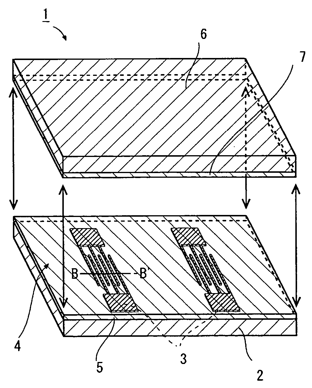
[0035] A first embodiment will be described, with reference to FIG. 5. FIG. 5 is an exploded perspective view of an elastic boundary wave device 1 in accordance with the first embodiment. FIG. 6 is a cross-sectional view taken along a line B-B′ shown in FIG. 5. A description will be given under the assumption that the elastic boundary wave device 1 has the purpose of processing high frequency signals in a frequency range of 1 GHz.

[0036] Referring to FIGS. 5 and 6, the elastic boundary wave device 1 includes a first substrate 2 that is a piezoelectric substrate, comb-like electrodes (IDTs) 3 that are arranged on a main surface of the first substrate 2, a first dielectric film 5 that covers the IDTs 3 and that has a smoothed surface 4, a silicon-based second substrate 6, and a second dielectric film 7 provided on a main surface of the second substrate 6. The sm...

second embodiment

[0060] A description will now be given of a second embodiment, with reference to the accompanying drawings in which the same components and configurations as those of the first embodiment have the same reference numerals and a detailed explanation will be omitted, if not otherwise specified.

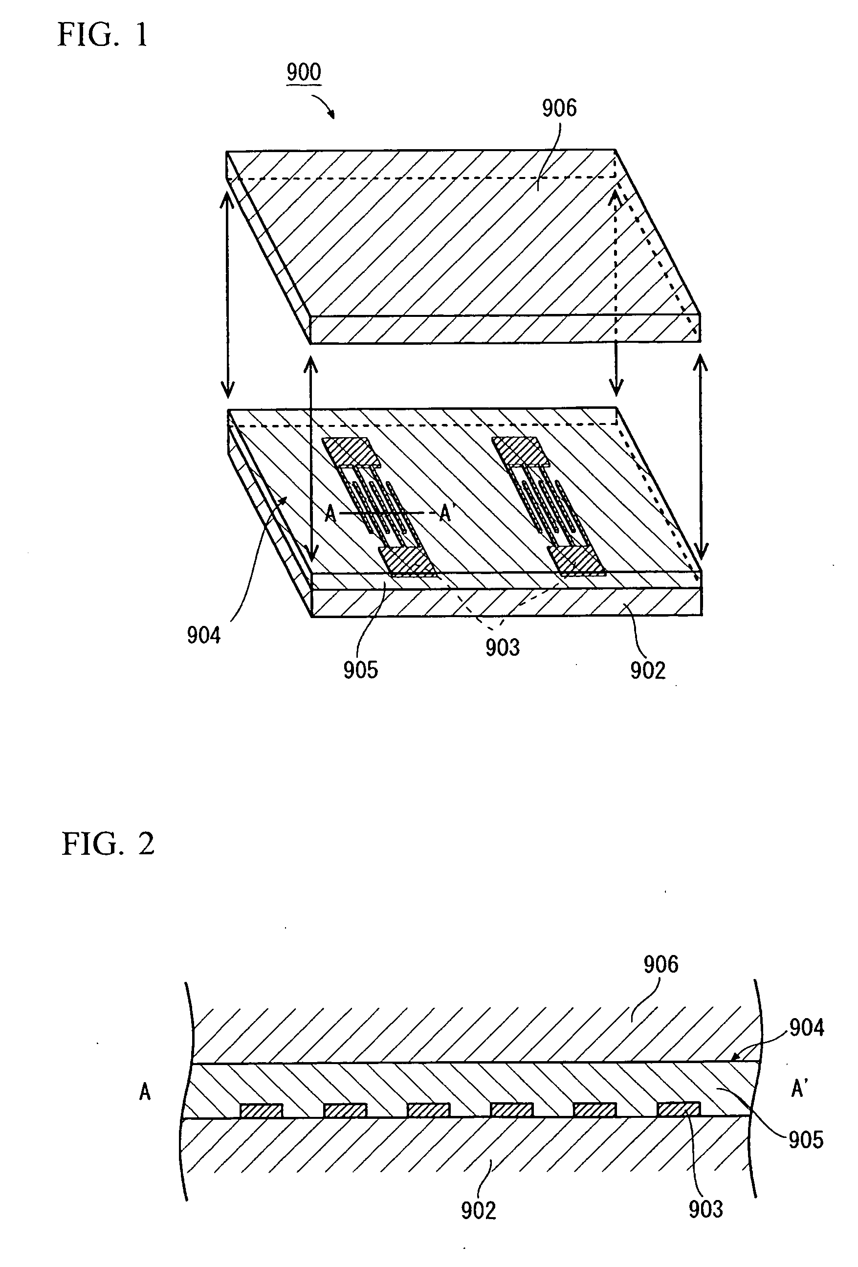
[0061]FIG. 9 is an exploded perspective view of an elastic boundary wave device 10 in accordance with the second embodiment of the present invention. FIG. 10 is a cross-sectional view taken along a line C-C′ shown in FIG. 9. The following description is directed to the elastic boundary wave device 10 for high frequency signals in the 1 GHz band.

[0062] Referring to FIGS. 9 and 10, the elastic boundary wave device 10 includes the first piezoelectric substrate 2, IDTs 3 arranged on the main surface of the first substrate 2, a dielectric film 15 that covers the IDTs 3 and has a smoothed surface 4, a silicon-based thin film 16 provided on a surface of the dielectric film 15, and the silicon-based se...

third embodiment

[0075] A description will now be given of a third embodiment of the present invention in which the same components and configurations as those of the first and second embodiments have the same reference numerals and a detailed explanation will be omitted, if not otherwise specified.

[0076]FIG. 9 also shows an elastic boundary wave device 20 of the third embodiment. FIG. 12 is a cross-sectional view taken along a line D-D′ shown in FIG. 9. The following description is directed to the elastic boundary wave device 20 for high frequency signals in the 1 GHz band.

[0077] Referring to FIGS. 9 and 12, the elastic boundary wave device 20 includes the first piezoelectric substrate 2, the IDTs 3 on the main surface of the first substrate 2, a dielectric film 25 that covers the IDTs 3, a silicon-based thin film 26 that is provided on the surface of the dielectric film 25 and that has the smoothed surface 4, and the silicon-based second substrate 6. The silicon-based thin film 26 and the second...


PUM


Abstract

An elastic boundary wave device includes a first piezoelectric substrate, IDTs arranged thereon, a first dielectric film having a smoothed surface that covers the IDTs, a second substrate that is a silicon-based substrate, and a second dielectric film provided on a main surface of the second substrate. The smoothed surface of the first dielectric surface and a surface of the second dielectric film are joined together.

Description

BACKGROUND OF THE INVENTION [0001] 1. Field of the Invention [0002] This invention generally relates to an elastic boundary wave device and a method of manufacturing the same, and more particularly, to an elastic boundary wave device employed for a filter or oscillator on a television set, cellular phone, or PHS (Personal Handyphone System), and a method of manufacturing the same. [0003] 2. Description of the Related Art [0004] Conventionally, a surface acoustic wave device (hereinafter referred to as SAW device) has been known well as one of the devices that utilize elastic waves. The SAW device is employed in various types of circuits on devices that send and receive wireless signals, for instance, in a frequency range of 45 MHz to 2 GHz. Examples of the above-mentioned various types of circuits are a bandpass filter for transmission and reception, local oscillation filter, antenna duplexer, IF filter, and FM modulator. [0005] The SAW device utilizes elastic waves that travel on a...

Claims


Application Information

Patent Timeline
Patent Type & Authority Applications(United States)
IPC IPC(8): H01L41/09H01L41/18H01L41/22H03H3/08H03H9/02H03H9/145H03H9/25
CPCH03H9/0222H03H3/08H03H9/25
Inventor MISHIMA, NAOYUKIMIURA, MICHIO
Owner TAIYO YUDEN KK
Why Eureka
Try Eureka