Manufacturing method of image sensor device

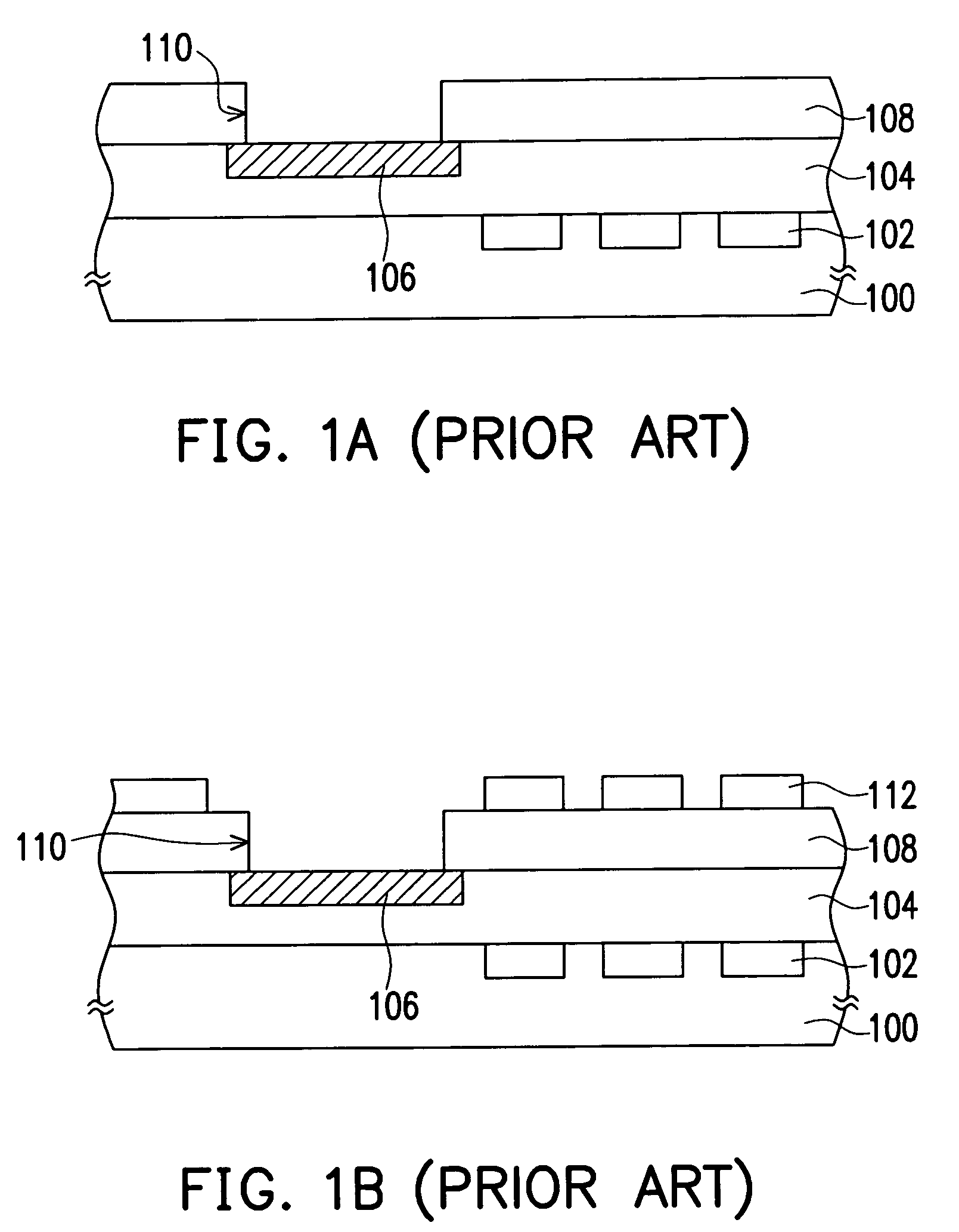
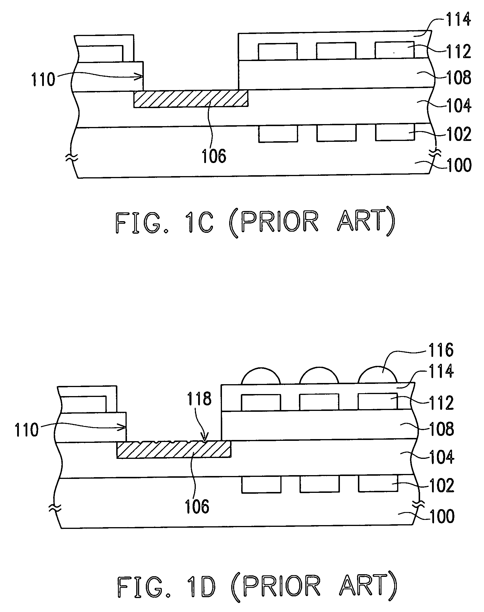
a manufacturing method and image sensor technology, applied in the direction of semiconductor devices, basic electric elements, electrical equipment, etc., can solve the problems of poor electrical contact between the wires and the bonding pads, adverse influence on the wiring process of the package, peeling of the wires, etc., to avoid corrosion and ensure the wiring process.

Inactive Publication Date: 2005-05-12
UNITED MICROELECTRONICS CORP
View PDF7 Cites 24 Cited by
  • Summary
  • Abstract
  • Description
  • Claims
  • Application Information

AI Technical Summary

Benefits of technology

[0013] Accordingly, one object of the present invention is to provide a manufacturing method of an image sensor device, such that the surface of the bonding pad avoided from corrosion due to chemical solution of the photoresist and developer, so that a reliable wiring process can be carried out.

Problems solved by technology

The existence of the pits 118 will adversely influence the wiring process of the package, and generally results in, for example, peeling of the wires, or poor electrical contact between the wires and the bonding pads.

Method used


Image

  • Manufacturing method of image sensor device
  • Manufacturing method of image sensor device
  • Manufacturing method of image sensor device

Examples


Embodiment Construction

[0023] The present invention now will be described more fully hereinafter with reference to the accompanying drawings, in which preferred embodiments of the invention are shown. This invention may, however, be embodied in many different forms and should not be construed as limited to the embodiments set forth herein; rather, these embodiments are provided so that this disclosure will be thorough and complete, and will fully convey the scope of the invention to those skilled in the art. Like numbers refer to like elements throughout.

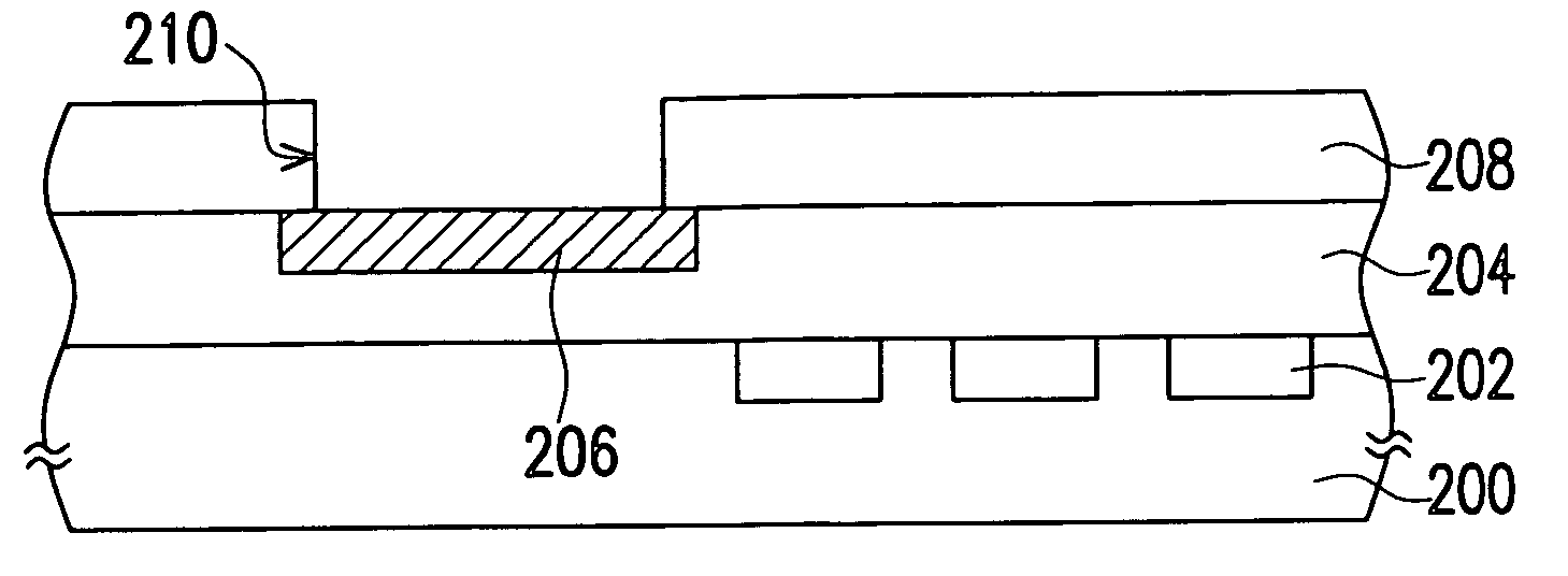
[0024]FIG. 2A to FIG. 2F are cross-sectional views schematically illustrating a manufacturing process of an image sensor device according to a preferred embodiment of the present invention. Hereinafter, in order to simplify the description, parts of the components and the corresponding descriptions in the manufacturing process are omitted.

[0025] First of all, referring to FIG. 2A, a substrate 200 is provided, and a plurality of photodiode sensing areas ...


PUM


Abstract

A manufacturing method of image sensor device is provided. The image sensor device is suitable for a substrate having at least one bonding pad. Wherein a plurality of photodiode sensing areas are formed on the substrate, at least a dielectric layer is formed over the substrate and the bonding pad is disposed in the dielectric layer. Wherein a first cover layer having an opening is disposed over the dielectric layer, wherein a portion of the bonding pad is exposed within the opening, forming a second cover layer over the first cover layer and the opening, and forming color filters over the second cover layer, then forming a planarization layer over the second cover layer and the color filters, and forming a plurality of micro lenses over the planarization layer.

Description

CROSS-REFERENCE TO RELATED APPLICATION [0001] This application claims the priority benefit of Taiwan application serial no. 92131626, filed on Nov. 12, 2003, the full disclosure of which is incorporated herein by reference. BACKGROUND OF THE INVENTION [0002] 1. Field of the Invention [0003] The present invention is generally related to a manufacturing method of an image sensor device. More particularly, the present invention relates to a manufacturing method of an image sensor device for preventing the generation of a pit on a surface of the bonding pad. [0004] 2. Description of the Related Art [0005] Conventionally, a charge coupled device (CCD) is generally used for a solid-state image sensor since the property of high dynamic range, low dark current, and well developed technology. However, in recent years, since a complementary metal oxide semiconductor (CMOS) image sensor (CMOS Image Sensor, “CIS”) is substantially developed for being compatible with the manufacturing process of...

Claims


Application Information

Patent Timeline
Patent Type & Authority Applications(United States)
IPC IPC(8): H01L21/00H01L21/8238
CPCH01L27/14627H01L27/14621
Inventor CHEN, WEI-SHIAUHSIEH, FREDDY
Owner UNITED MICROELECTRONICS CORP
Why Eureka
Try Eureka