Transistor of semiconductor device, and method for manufacturing the same

a semiconductor device and transistor technology, applied in the direction of semiconductor devices, bulk negative resistance effect devices, electrical apparatus, etc., can solve the problems of short channel effect, leakage current generation, short channel effect, and almost double refresh time of dram, and achieve high device integration and speed

Inactive Publication Date: 2005-05-19
SK HYNIX INC
View PDF11 Cites 85 Cited by
  • Summary
  • Abstract
  • Description
  • Claims
  • Application Information

AI Technical Summary

Benefits of technology

[0008] Accordingly, it is an object of the present invention to provide a transistor of a semiconductor device and a method for forming the same wherein capacitance generated by junction leakage current and junction depletion in a source / drain junction layer is remove to achieve a high speed and high integration of the device.

Problems solved by technology

However, the refresh time of the DRAM is almost double in each generation because of a high speed and low power requirements.
However, the increase of the concentration of impurities results in increase of junction electric intensity, which generates short channel effects and leakage currents.
Moreover, the increase of concentration increases junction capacitance, thereby reducing the operation speed of the device.
As described above, in the conventional transistor of the semiconductor device and a method for manufacturing the same, the characteristics of the device is degradeddue to the increased concentration of impurities implanted into the substrate, thereby making the achievement of the high operation speed and high integration of the semiconductor device more difficult.

Method used


Image

  • Transistor of semiconductor device, and method for manufacturing the same
  • Transistor of semiconductor device, and method for manufacturing the same
  • Transistor of semiconductor device, and method for manufacturing the same

Examples


first embodiment

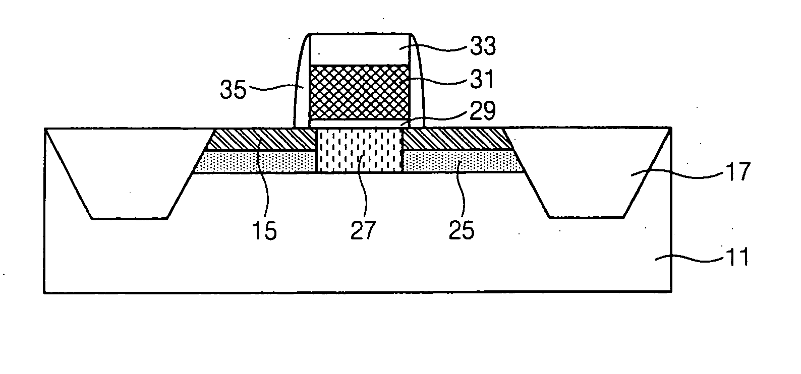
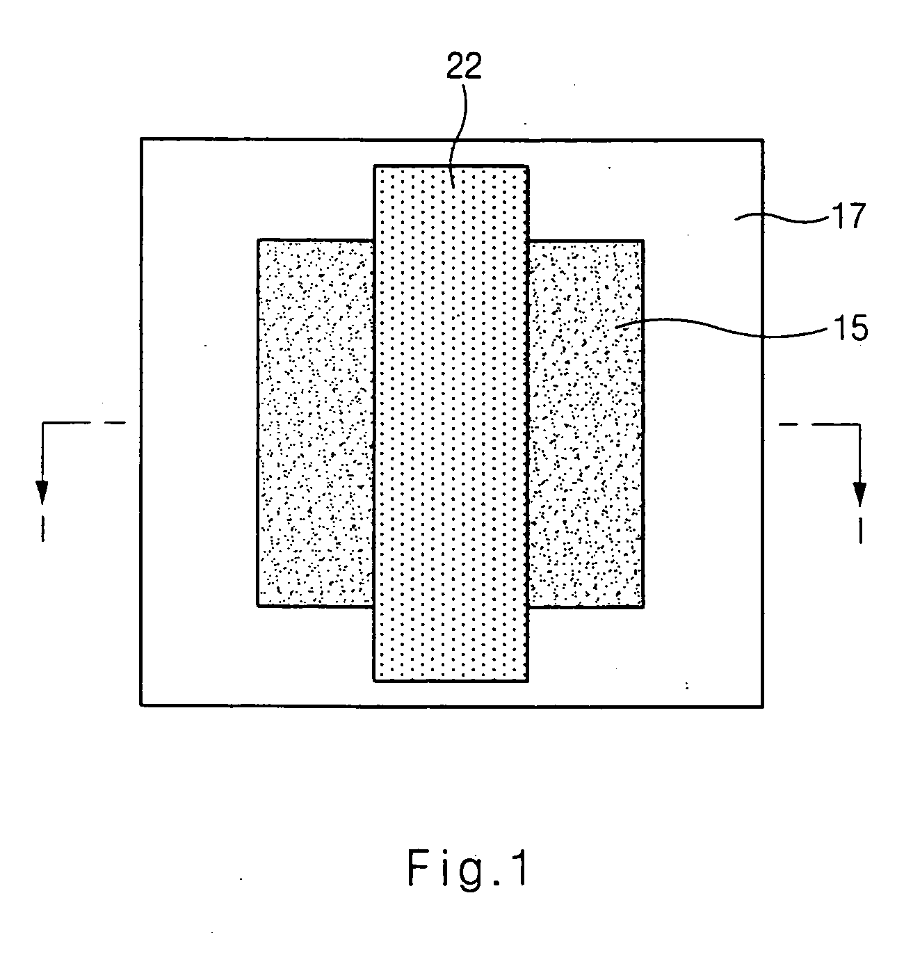
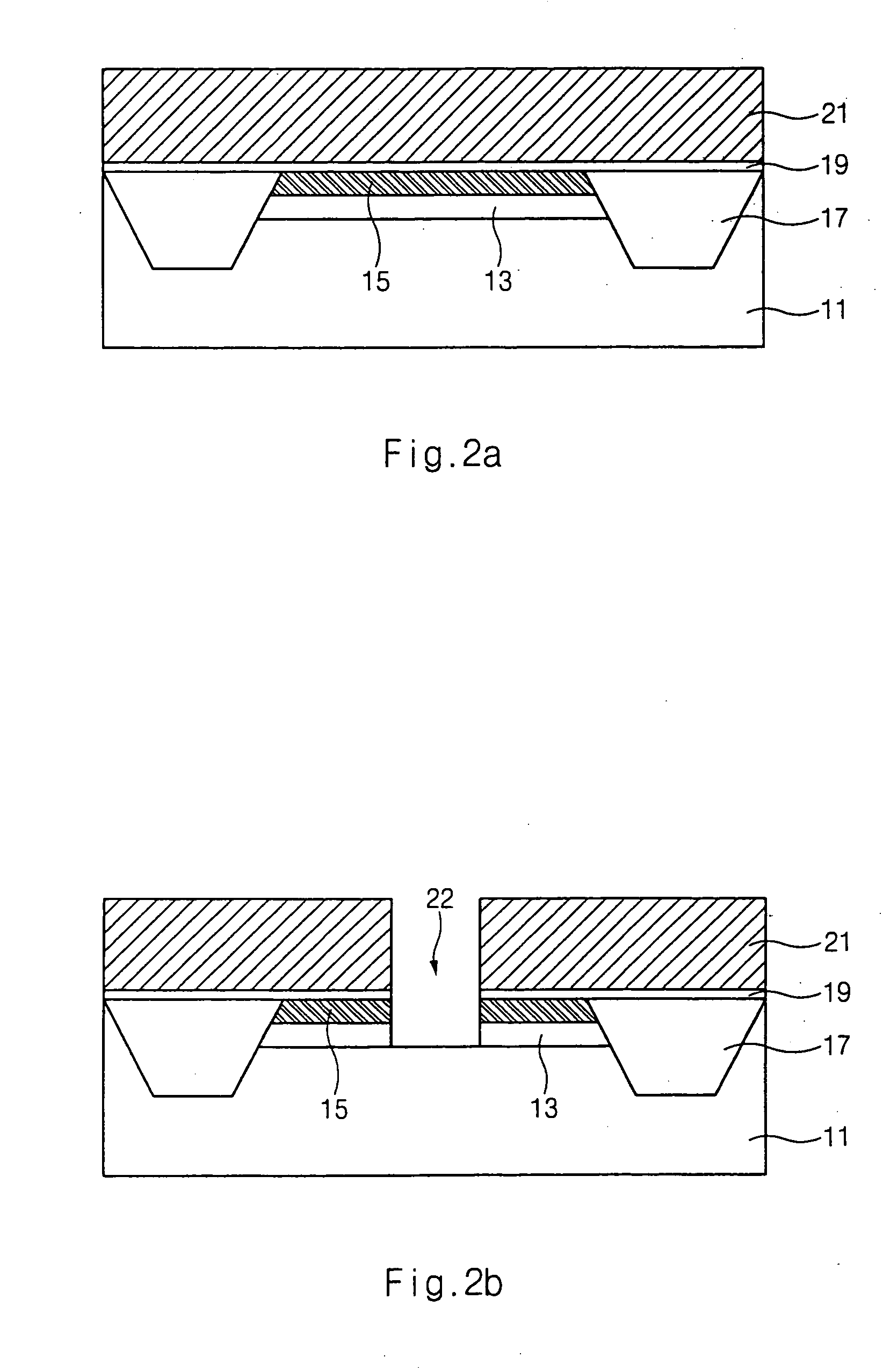
[0017]FIG. 1 is a layout diagram illustrating an active region and a gate electrode region 22 formed on a semiconductor substrate 11, and FIGS. 2a to 2f are cross-sectional diagrams illustrating sequential steps of a method for forming a transistor of a semiconductor device in accordance with the present invention, taken along lines I-I of FIG. 1.

[0018] Referring to FIG. 2a, an first epitaxial layer 13 and a conductive second epitaxial layer 15 are sequentially formed on the semiconductor substrate 11 consisting of silicon.

[0019] Preferably, the first epitaxial layer 13 is an epitaxial SiGe layer formed under an atmosphere of a mixture gas of a gas from the group consisting of GeH4, SiH4, SiH2Cl2 and combinations thereof, HCl and H2, and has a thickness ranging from 50 to 1000 Å, and the second epitaxial layer 15 is an epitaxial Si layer formed under an atmosphere of a gas from the group consisting of SiH4, SiH2Cl2 and combinations thereof, HCl and H2, and has a thickness ranging f...

second embodiment

[0038]FIGS. 3a to 3i are cross-sectional diagrams illustrating sequential steps of a method for forming a transistor of a semiconductor device in accordance with the present invention, taken along lines I-I of FIG. 1.

[0039] Referring to FIG. 3a, an first epitaxial layer 43 and a conductive second epitaxial layer 45 are sequentially formed on the semiconductor substrate 41 comprised of silicon. Preferably, the first epitaxial layer 43 is an epitaxial SiGe layer having a thickness ranging from 50 to 1000 Å formed under an atmosphere of a mixture gas of a gas from the group consisting of GeH4, SiH4, SiH2Cl2 and combinations thereof, HCl and H2, and the second epitaxial layer. 45 is an epitaxial Si layer having a thickness ranging from 50 to 1000 Å formed under an atmosphere of a mixture gas of a gas from the group consisting of SiH4, SiH2Cl2 and combinations thereof, HCl and H2.

[0040] A pad oxide film (not shown) and a nitride film (not shown) are sequentially formed on the entire sur...


PUM


Abstract

A semiconductor device and a method for forming the same are disclosed. The semiconductor device includes an epitaxial source / drain junction layer having an insulating film thereunder. The method comprises the step of forming a under-cut under an epitaxial source / drain junction layer so that an insulating film filling the under-cut can be formed.

Description

BACKGROUND OF THE INVENTION [0001] 1. Field of the Invention [0002] The present invention relates to transistor of semiconductor device and method for manufacturing the same, and more particularly to improved transistor of memory device and method for manufacturing the same which provides a high speed and high integrated device by preventing deterioration of the characteristics of the device resulting from increase of impurity concentration as the integration of the device is increased. [0003] 2. Description of the Background Art [0004] As the integration of a semiconductor device has been increased, integration of a DRAM has increased. However, the refresh time of the DRAM is almost double in each generation because of a high speed and low power requirements. [0005] As the density of a memory device continuously increases, the concentration of impurities implanted into a substrate must be increased to minimize short channel effects, threshold voltages and leakage currents. However,...

Claims


Application Information

Patent Timeline
Patent Type & Authority Applications(United States)
IPC IPC(8): H01L29/78H01L21/336H01L29/06
CPCH01L29/0653H01L29/66651H01L29/66621H01L29/66545H01L29/78
Inventor KWAK, BYUNG ILAHN, KYUNG JUN
Owner SK HYNIX INC
Why Eureka
Try Eureka