
Method of forming minimally spaced word lines

a technology of word lines and lithography, which is applied in the direction of semiconductor devices, semiconductor/solid-state device details, electrical devices, etc., can solve the problems of inability of the process to achieve a minimum space or minimal critical dimension (cd) between two adjacent word lines and, consequently, between two adjacent memory cells, and current lithography technologies cannot afford these values,

Inactive Publication Date: 2005-05-19
JUENGLING WERNER
View PDF39 Cites 16 Cited by
  • Summary
  • Abstract
  • Description
  • Claims
  • Application Information

AI Technical Summary

Benefits of technology

"The present invention provides a double exposure photolithography technique for fabricating minimally spaced word lines of a memory cell array. This technique involves forming multiple gate stack layers over a semiconductor substrate and creating small trenches between them using a first mask. The small trenches are then filled with a filler material and a second mask is used to pattern and etch the adjacent gate stack layers. After removal of the filler material, the gate stacks remain minimally spaced on the substrate. This technique allows for a more efficient use of space in the memory cell array and improves performance."

Problems solved by technology

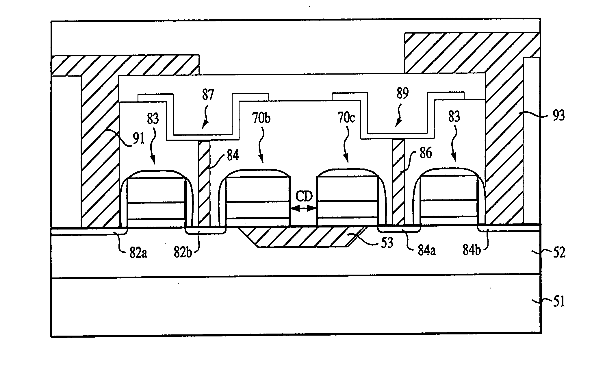
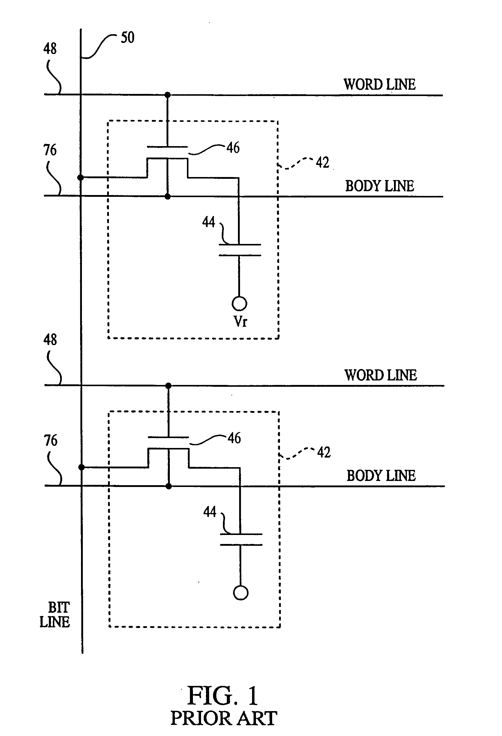
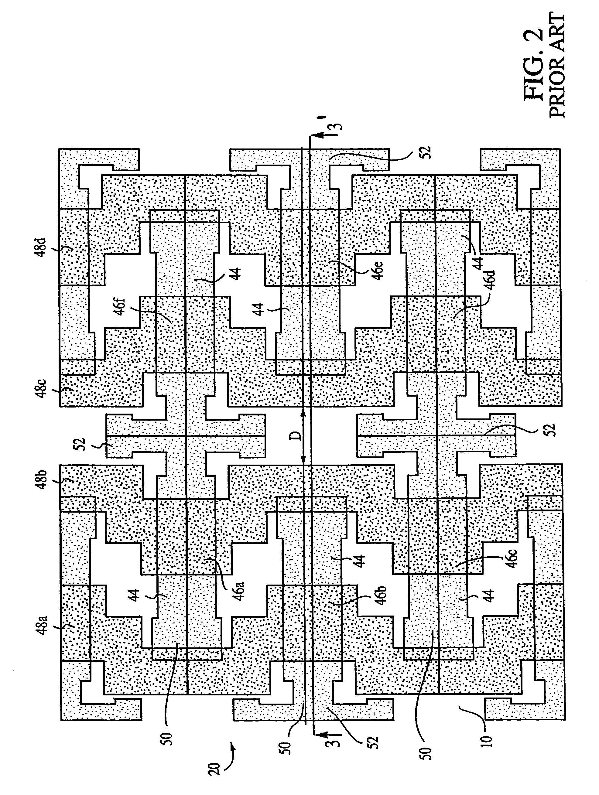
A drawback of conventional DRAM fabrication is the inability of the process to achieve a minimal space or minimal critical dimension (CD) between two adjacent word lines and, consequently, between two adjacent memory cells.
With increasing packing density of DRAM cells, it is desirable for the distance D (FIGS. 2-3) to decrease to values below 500 Angstroms, and preferably to less than or equal to 300 Angstroms, or even less than 100 Angstroms, but current lithography technologies do not afford these values.
However, these cells are expensive and difficult to fabricate because the structure of the array devices is typically incompatible with that of the non-array devices.

Method used


Image

  • Method of forming minimally spaced word lines
  • Method of forming minimally spaced word lines
  • Method of forming minimally spaced word lines

Examples


Embodiment Construction

[0042] In the following detailed description, reference is made to various exemplary embodiments of the invention. These embodiments are described with sufficient detail to enable those skilled in the art to practice the invention, and it is to be understood that other embodiments may be employed, and that is structural and electrical changes may be made without departing from the spirit or scope of the present invention.

[0043] The term “substrate” used in the following description may include any semiconductor-based structure that has an exposed semiconductor surface. Structure must be understood to include silicon, silicon-on insulator (SOI), silicon-on sapphire (SOS), doped and undoped semiconductors, epitaxial layers of silicon supported by a base semiconductor foundation, and other semiconductor structures. The semiconductor need not be silicon-based. The semiconductor could be silicon-germanium, germanium, or gallium arsenide. When reference is made to substrate in the follow...


PUM


Abstract

A method of forming minimally spaced word lines is disclosed. A double exposure technique is employed at the gate formation level. A small trench is defined through gate stack layers by using a tapered etch or spacers to achieve the desired width of the trench. A filler material fills the trench and forms a filler plug. The gate layers adjacent to the trench are then patterned and etched and the filler plug is removed to obtain gate stacks spaced apart by a distance of less than about 400 Angstroms.

Description

FIELD OF THE INVENTION [0001] The present invention relates to an improved semiconductor structure for high density device arrays, and in particular to a DRAM cell array and a process for its formation. BACKGROUND OF THE INVENTION [0002] Two major types of random access memory cells—dynamic and static—are currently used in the semiconductor industry. Dynamic random-access memories (DRAM) can be programmed to store a voltage which represents one of two binary values, but require periodic reprogramming or “refreshing” to maintain this voltage for more than very short time periods. Static random-access memory are so called because they do not require periodic refreshing. [0003] DRAM memory circuits are manufactured by replicating millions of identical circuit elements, known as DRAM cells, on a single semiconductor wafer. Each DRAM cell is an addressable location that can store one bit (binary digit) of data. In its most common form, a DRAM cell consists of two circuit components, a fi...

Claims


Application Information

Patent Timeline
Patent Type & Authority Applications(United States)
IPC IPC(8): H10B12/00
CPCH01L27/10811H01L27/10891H01L27/10873H10B12/312H10B12/05H10B12/488
Inventor JUENGLING, WERNER
Owner JUENGLING WERNER
Learn More