Multi-chip module

a multi-chip module and chip technology, applied in the field of multi-chip modules, can solve the problems of reducing the distance between the semiconductor chip and the wiring distance, and the device becomes limited naturally, so as to achieve the effect of reducing the size and double the circuit performan

Active Publication Date: 2005-05-19
RENESAS ELECTRONICS CORP
View PDF5 Cites 48 Cited by
  • Summary
  • Abstract
  • Description
  • Claims
  • Application Information

AI Technical Summary

Benefits of technology

[0012] The first semiconductor chip laid out over the surface of the substrate can omit an area larger than the first semiconductor chip therefrom. The area is used to connect the first semiconductor chip to a favorable signal transmission path realized over the substrate. The substrate is thus reduced in size. In addition, the second and third semiconductor chips are connected to the substrate under the same condition, thereby the circuit performance is doubled.

Problems solved by technology

However, if a plurality of semiconductor devices, each being packaged independently with use of an ordinary packaging technique employed for QFP (Quad Flat Package), CSP (Chip Size Package or Chip Scale Package), and BGA (Ball Grid Array) are to be mounted on such a substrate as a printed wired substrate instead of using a plurality of semiconductor chips, it is difficult to reduce the distance between semiconductor chips and their wiring distances, so that the signal delay is promoted by the wiring, thereby the devices come to be limited naturally in realization of faster operations and smaller sizes.

Method used


Image

  • Multi-chip module
  • Multi-chip module
  • Multi-chip module

Examples


Embodiment Construction

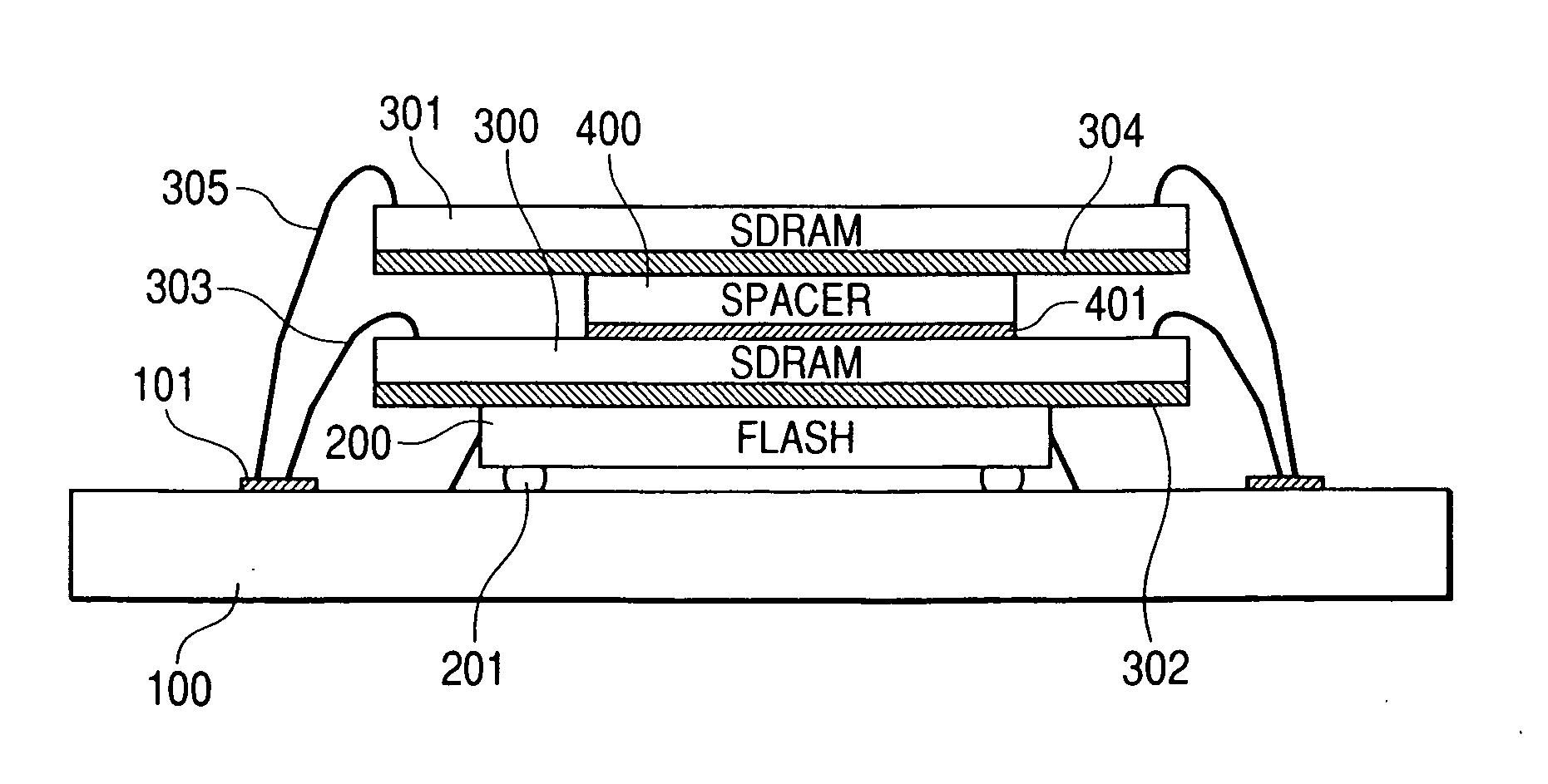
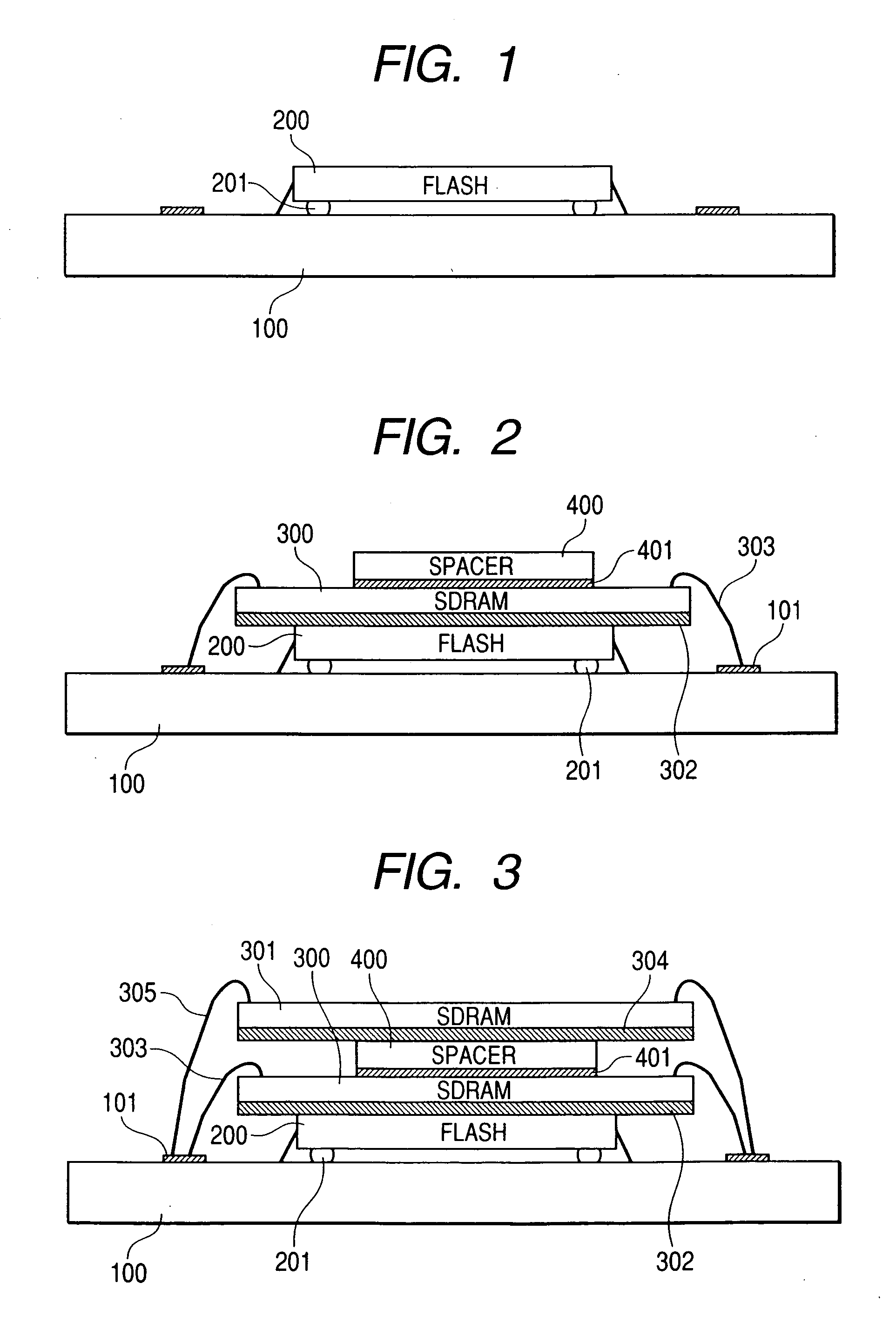
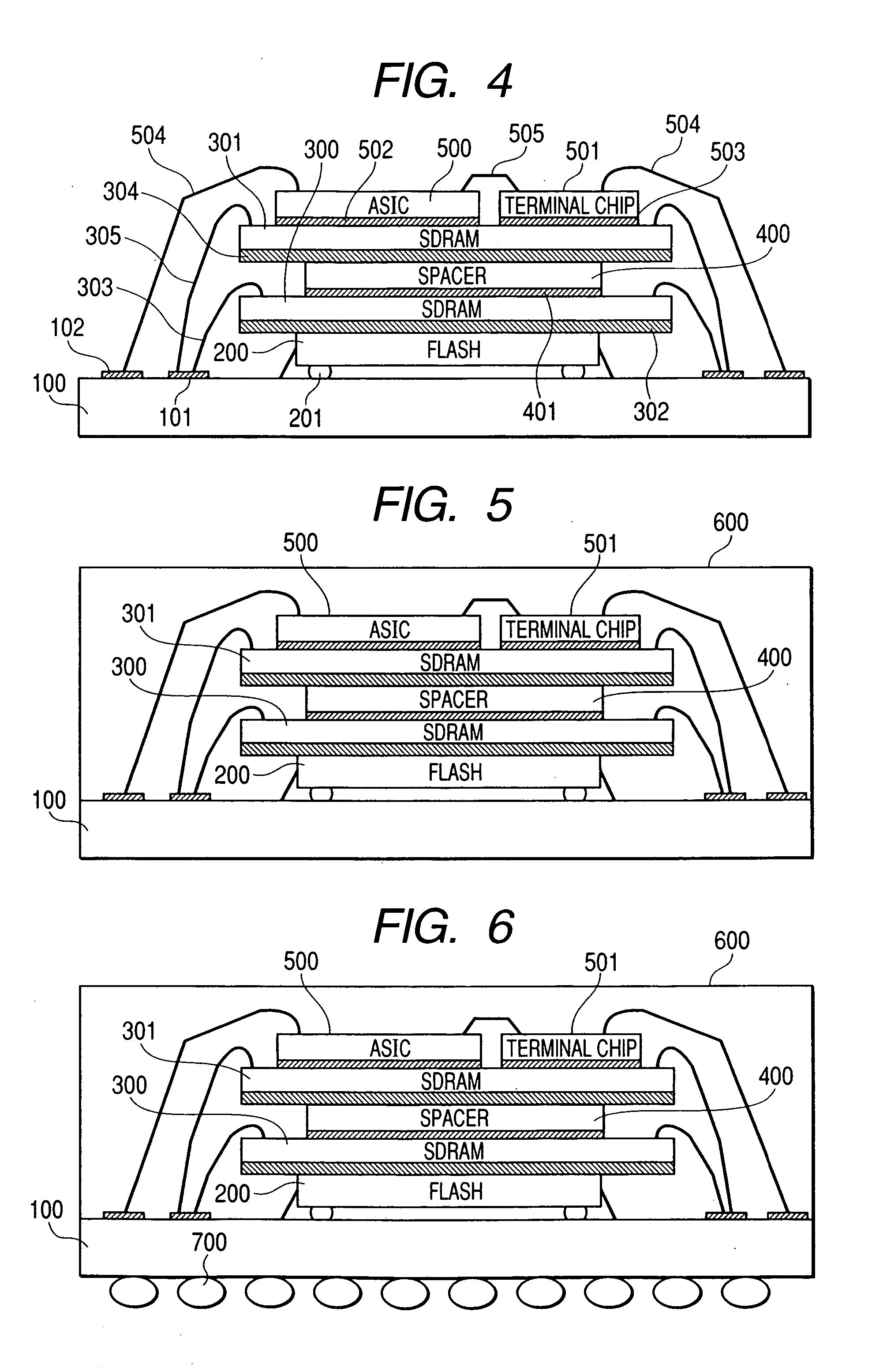
[0028]FIGS. 1 through 6 show cross sectional views of a multi-chip module in an embodiment of the present invention. In FIGS. 1 through 6, how to assemble the multi-chip module is shown as an assembly flowchart. The multi-chip module in this embodiment is configured by application specified integrated circuits, that is, a microcomputer LSI that includes a CPU composed of a specific purpose IC (hereinafter, to be referred to simply as ASIC), two synchronous dynamic random access memories (hereinafter, to be referred to simply as SDRAM respectively), and a flash EEPROM (Flash Electrically Erasable and Programmable Read Only Memory; hereinafter, to be referred to simply as FLASH) therein. Those components are stacked in the module.

[0029] Although not restricted specially, the sizes of the semiconductor chips to be stacked in the module will be as follows: the ASIC 500 is 5.75×5.75; the SDRAM 300 / 301 is 6.84×6.80; and the FLASH 200 is 8.51×5.82. The SDRAM 300 / 301 has a storage capacity...


PUM


Abstract

Disclosed here is a multi-chip module enhanced in performance and reduced in size. A second semiconductor chip having bonding pads at the periphery of its surface is mounted over a first semiconductor chip laid out over a surface of a substrate back to back and a spacer is provided at a portion of the second semiconductor chip surface except for a predetermined area that includes the portion where the bonding pads are formed while a third semiconductor chip is mounted over the spacer, the third semiconductor having the same circuit function as the second semiconductor chip and oriented similarly to the second semiconductor chip. The bonding pads of the second and third semiconductor chips are connected to their corresponding electrodes formed over the substrate through bonding wires respectively, then the first to third semiconductor chips and the bonding wires provided over the substrate are all sealed by a sealing agent.

Description

CROSS-REFERENCE TO RELATED APPLICATION [0001] The present invention claims priority from Japanese patent application No. 2003-387188 filed on Sep. 17, 2003, the content of which is hereby incorporated by reference into this application. BACKGROUND OF THE INVENTION [0002] The present invention relates to a multi-chip module (MCM), particularly to a technique to be applied effectively to a multi-chip module structured so that a plurality of semiconductor chips, each having a function different from those of others, are mounted on one substrate, thereby the multi-chip module is configured as one semiconductor integrated circuit device. [0003] According to the so-called multi-chip module technique, a plurality of semiconductor chips are mounted on one substrate provided with a plurality of internal wired lines and a plurality of external terminals so that those semiconductor chips are united with the substrate into one integrated circuit device. For such an integrated circuit device, Ja...

Claims


Application Information

Patent Timeline
Patent Type & Authority Applications(United States)
IPC IPC(8): H01L25/18H01L25/065H01L25/07H01L27/14
CPCH01L23/3121H01L25/18H01L2224/32225H01L2224/45144H01L2924/01021H01L2924/30107H01L2924/15311H01L2924/1433H01L2924/14H01L2924/01079H01L2225/06575H01L2225/06517H01L2225/0651H01L2224/73265H01L2224/73204H01L2224/73203H01L2224/49171H01L2224/48227H01L2224/48137H01L2224/32145H01L2224/16225H01L2924/00H01L2924/00012H01L2924/00014H01L24/73H01L2224/05571H01L2224/05573H01L2224/73253H01L2224/05599
Inventor KURODA, HIROSHIISHIDA, SHINPEI
Owner RENESAS ELECTRONICS CORP
Why Eureka
Try Eureka