
Bimorph MEMS devices

Inactive Publication Date: 2005-05-19
PALO ALTO RES CENT INC
View PDF25 Cites 15 Cited by
  • Summary
  • Abstract
  • Description
  • Claims
  • Application Information

AI Technical Summary

Benefits of technology

[0052]FIG. 29B shows the bimorph bonded to a conductive surface

Problems solved by technology

However, antiferroelectric / antiferroelectric bimorph macro-world sized structures are not available due in part to the described nature of antiferroelectric material.
MEMS-type bimorphs have not been developed due at least in part to manufacturing obstacles related to building two piezoelectric or antiferroelectric thin or thick film layers together, or in combination with each other.
A further obstacle is developing a system which is able to pole the piezoelectric layers with suitable directions, and to make antiferroelectric / antiferroelectric bimorphs move along two directions.
Due to the dampening effect, the bimorphs created by this process, are not as efficient as “true” bimorphs made by direct bonding of two films or layers together.
The state of the art does not provide an efficient high-yield process for the manufacture of true bimorph-based structures in the MEMS scale, where the layers are piezoelectric / piezoelectric, antiferroelectric / antiferroelectric or antiferroelectric / piezoelectric combinations.
Also, usable antiferroelectric / antiferroelectric macro-sized bimorph structures are not now available.
This is due at least in part to current film production processes which fail to provide an efficient manner of producing piezoelectric films within this range, and therefore no consideration has been given to making two-layer thick films together in this range.

Method used


Image

  • Bimorph MEMS devices
  • Bimorph MEMS devices
  • Bimorph MEMS devices

Examples


Embodiment Construction

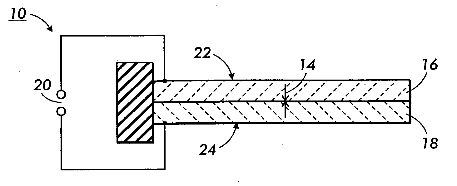
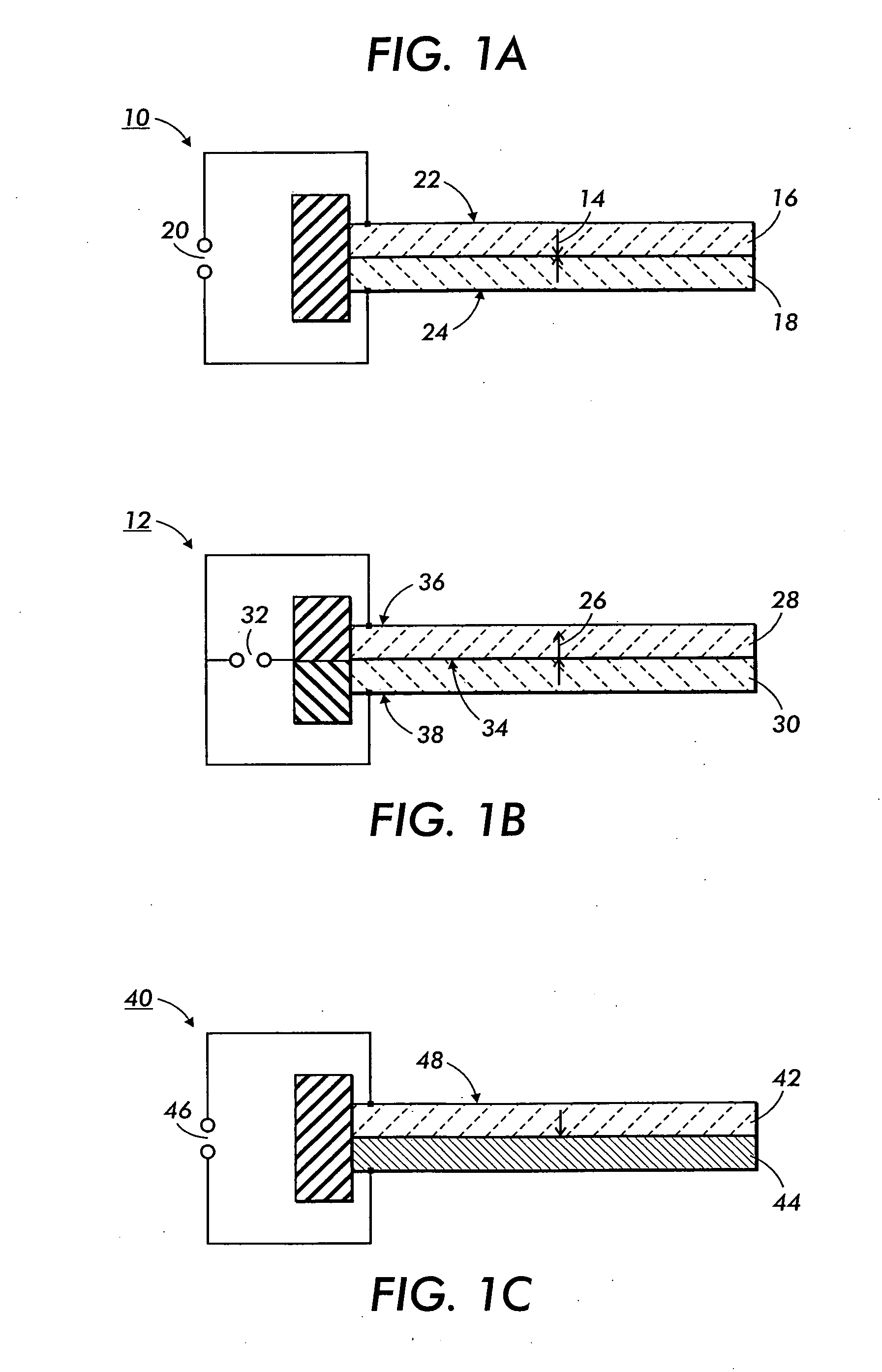
[0060] In consideration of the discussion in connection with FIGS. 1A-1C, the combination of piezoelectric materials and MEMS technologies, has permitted the development of thin film (with film thickness usually between 1 to 10 μm) type MEMS unimorph cantilevers and diaphragms on silicon substrates. Among other uses, cantilever unimorphs have been used as sensors such as accelerometers and force sensors for atomic force microscope (AFM). Diaphragm unimorphs have been used, for example, as acoustic sensors such as sonar and actuators such as for pumping or ejecting fluid via micro-pumps. The piezoelectric thin films, usually PZT, for such uses are made by sol-gel, sputtering, laser ablation, chemical vapor deposition or other appropriate process. The film thickness is less than 10 μm as these processes do not lend themselves to making thick films (with film thickness between 10 μm to 100 μm). On the other hand, as all these processes need to anneal the piezoelectric films at least ab...


PUM

PropertyMeasurementUnit
Thicknessaaaaaaaaaa
Thicknessaaaaaaaaaa
Thicknessaaaaaaaaaa

Abstract

A micro-electromechanical dimensioned bimorph structure includes a first element layer structure, and a second element layer structure. The element layer structures are provided in various combinations, including piezoelectric / piezoelectric, antiferroelectric / antiferroelectric or antiferroelectric / piezoelectric. The layer thickness of the element structure is less than 100 μm. A bonding layer bonds the first element structure directly to the second element structure and the bonding layer thickness is less than 10 μm. The bimorph structure can be made in various forms including a cantilever or a diaphragm. Microfluidic devices using the bimorph structures may also be constructed.

Description

BACKGROUND OF THE INVENTION [0001] Piezoelectric materials, especially piezoelectric ceramics such as PZT (lead zirocnate titanate) are the most widely known materials used for the manufacture of actuators, sensors and transducers among all ferroelectric-type materials (poled ferroelectric material is piezoelectric material). Recently, however, other materials have begun to be developed for use as actuators, sensors, and transducers, which have some beneficial properties not found in piezoelectric materials. One of these materials is an antiferroelectric material, such as antiferroelectric ceramics found in PZT or PZST (lead zirconate stannate titanate) systems. [0002] Antiferroelectric materials have anti-parallel dipoles which can be transferred into a parallel state (ferroelectric state) under an applied field, thus double hysteresis loops will appear on their P (polarization)-E (electric field) curve. A large strain (about 0.4% to 0.8%) accompanies an antiferroelectric-ferroelec...

Claims


Application Information

Patent Timeline
IPC IPC(8): H01L41/09H01L41/24H02N2/04
CPCB81B3/0024B81B2201/032H01L41/094H01L41/314H01L41/337H01L41/22Y10T29/49147Y10T29/49156Y10T29/49126Y10T29/42Y10T29/49155Y10T29/4913Y10T29/49128H01L41/313H10N30/2042H10N30/01H10N30/073H10N30/074H10N30/086
Inventor XU, BAOMINWONG, WILLIAM S.
Owner PALO ALTO RES CENT INC
Learn More