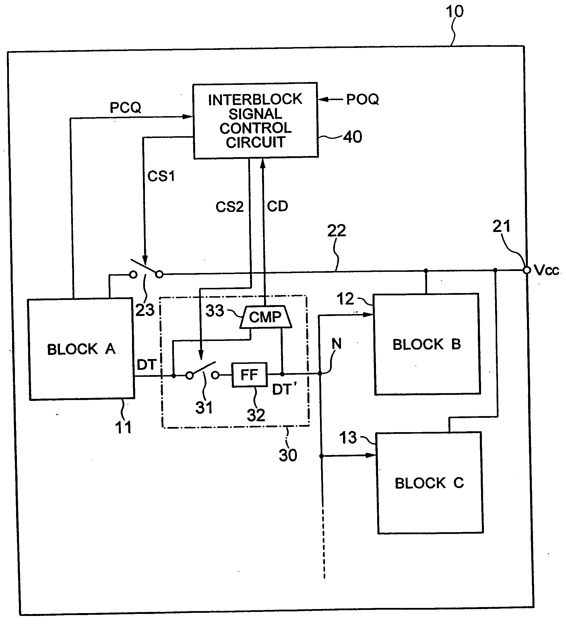
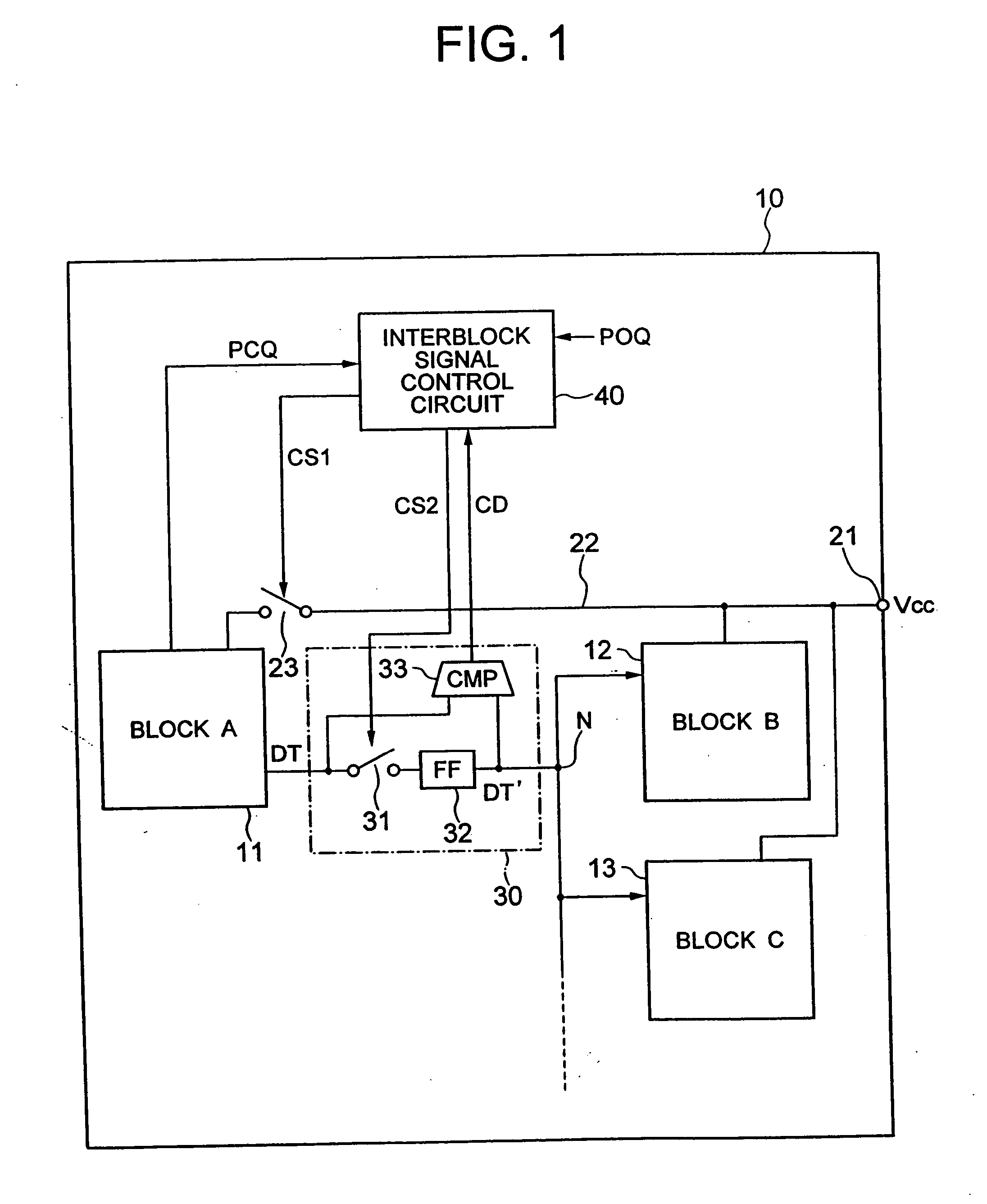
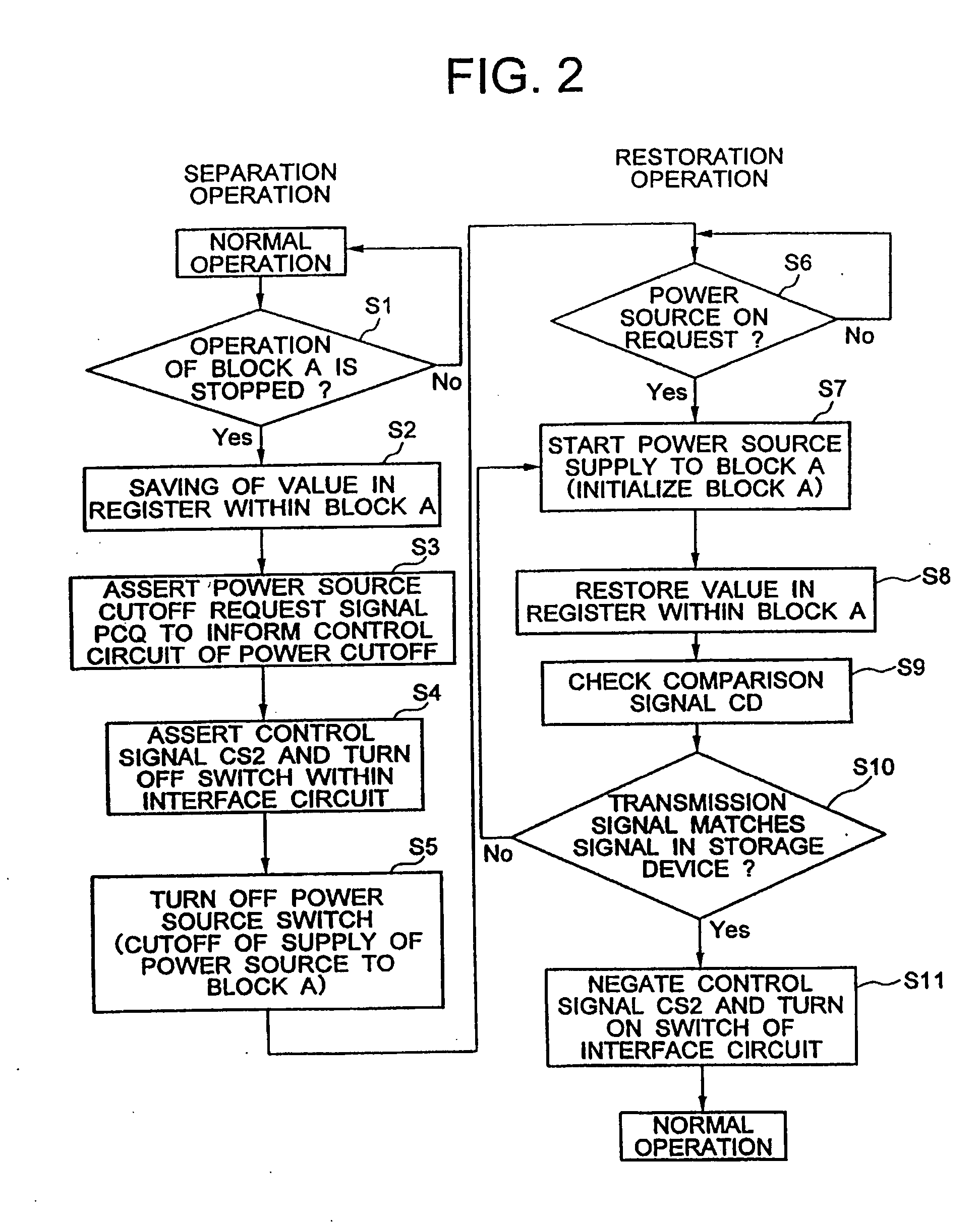
Multiple circuit blocks with interblock control and power conservation
a technology of interblock control and multi-circuit blocks, applied in the field of reducing power consumption of semiconductor integrated circuits, can solve the problems of malfunction of such circuits, insufficient power consumption reduction, and complex design of such circuits, and achieve the effect of reducing power consumption
- Summary
- Abstract
- Description
- Claims
- Application Information
AI Technical Summary
Benefits of technology
Problems solved by technology
Method used
Image

Examples
first embodiment
[0040] While above, the description has been given with respect to the first embodiment in which the interblock signal control circuit 40 controls the cutoff of the supply of the power source voltage to the circuit block 11, the present invention can also be applied to an embodiment in which the power source voltage to the circuit block 11 is supplied from the outside separately from other circuit blocks, and the cutoff of the supply of the power source voltage to the circuit block 11 is carried out in the outside.
second embodiment
[0041] Next, the present invention will hereinbelow be described with reference to FIG. 5. In FIG. 5, the same circuits and portions as those in FIG. 1 are designated with the same reference numerals, and the repeated description is omitted here for the sake of simplicity. In the figure, reference numeral 50 designates an external power source device.
[0042] The second embodiment is such that power source switches 23A, 23B and 23C are provided to be able to cut off the supply of the power source voltages to a plurality of circuit blocks 11, 12, and 13 on a semiconductor chip 10, respectively. While not particularly limited, power source line areas 60A, 60B and 60C having power source lines distributed therein are respectively provided in the peripheries of the circuit blocks 11, 12 and 13, and interface areas 30A, 30B and 30C in each of which a plurality of interface circuits 30s each shown in FIG. 1 are respectively provided in the outside of the power source line areas 60A, 60B and...
fourth embodiment
[0058]FIG. 8 shows a configuration of a semiconductor IC to which the present invention is applied.
[0059] The present embodiment of the semiconductor IC is configured in such a way that when the internal circuit has the circuit block 11 for which the supply of the power source voltage is cut off in accordance with the operation mode and the circuit block 12 which has the power source voltage supplied thereto at all times to be operated, an I / O circuit is divided into an I / O part 131 in which the supply of the power source voltage is cut off in correspondence to the circuit blocks and an I / O part 132 which has the power source voltage supplied thereto at all times to be operated. An interface area 30A in which a plurality of interface circuits 30 as shown in FIG. 1 are arranged is formed between the circuit block 11 and the circuit block 12.
[0060] In addition, the present embodiment of the semiconductor IC is also configured in such a way that the signal(s), which does(do) not need ...
PUM
 Abstract
Description
Claims
Application Information
 - R&D
- Intellectual Property
- Life Sciences
- Materials
- Tech Scout
- Unparalleled Data Quality
- Higher Quality Content
- 60% Fewer Hallucinations
Browse by: Latest US Patents, China's latest patents, Technical Efficacy Thesaurus, Application Domain, Technology Topic, Popular Technical Reports.
© 2025 PatSnap. All rights reserved.Legal|Privacy policy|Modern Slavery Act Transparency Statement|Sitemap|About US| Contact US: help@patsnap.com