Memory module, memory chip, and memory system

a memory module and memory chip technology, applied in the field of memory modules, can solve the problems of significant waveform distortion, increased time constant of signal reflection, and significant waveform distortion, and achieve the effect of memory capability with reliability and reducing waveform distortion

Inactive Publication Date: 2005-05-19
LONGITUDE SEMICON S A R L
View PDF1 Cites 90 Cited by
  • Summary
  • Abstract
  • Description
  • Claims
  • Application Information

AI Technical Summary

Benefits of technology

[0025] The configuration of the memory module of the present invention allows for reducing the waveform ...

Problems solved by technology

The above-described known memory module has a problem that the waveforms thereof are significantly distorted due to a high-speed signal.
The problem is caused by the con...

Method used


Image

  • Memory module, memory chip, and memory system
  • Memory module, memory chip, and memory system
  • Memory module, memory chip, and memory system

Examples


first embodiment

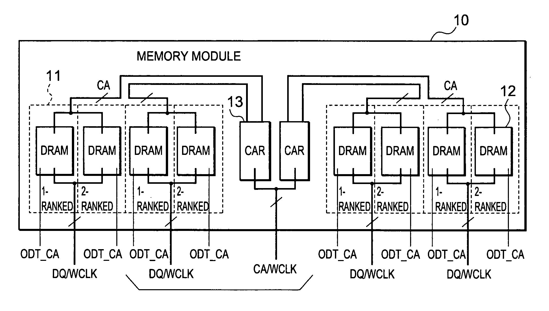
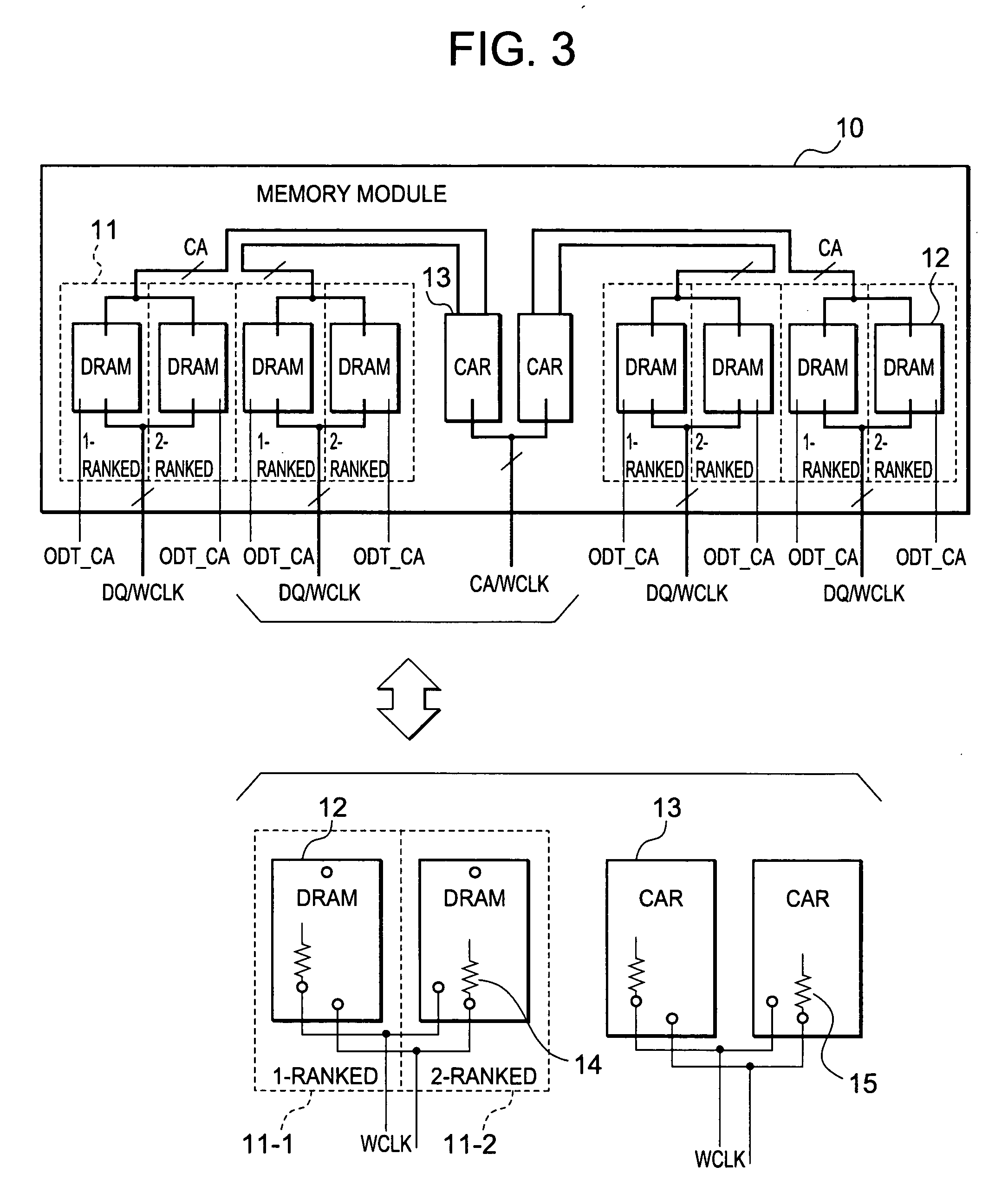
[0055]FIG. 3 is a block wiring diagram illustrating the present invention. As shown in this drawing, a memory module 10 includes 11-1-ranked and 11-2-ranked devices that are accessible at the same time. These devices are sixteen dynamic random access memories (DRAMs) 12. These DRAMs 12 are divided into two groups formed on both faces of a module substrate and each of the two groups includes eight DRAMs 12. These eight DRAMs 12 are divided into four memory groups and each of the four memory groups includes two DRAMs. One of the two DRAMs is mounted on one face of the module substrate and the other is mounted on the other face thereof. These two DRAMs are commonly wired. Therefore, this drawing shows only eight DRAMs 12. That is to say, each of the memory groups is paired with the other memory group adjacent thereto. Further, the rank of one of each pair of the adjacent memory groups is different from that of the other.

[0056] Thus, according to this embodiment, one DRAM 12 on the top ...

second embodiment

[0084] the present invention will now be described with reference to FIGS. 14 to 19.

[0085] According to this embodiment, eighteen DRAMs 12 are used, as shown in FIG. 14. That is to say, two DRAMs 12 are added to the DRAMs 12 of the first embodiment. These two added DRAMs 12 are stacked on a predetermined 1-ranked DRAM 12 and a predetermined 2-ranked DRAM 12 being adjacent thereto and paired therewith, whereby two units of two DRAMs stacked on each other are formed. One of the two units of the stacked DRAMs 12 is provided on one face of the module substrate and a DRAM 12 is provided on the other face thereof so as to form a memory group. The other of the two units of the stacked DRAMs 12 on one face of the module substrate and another DRAM 12 on the other face thereof also form another memory group. According to this configuration, active termination is performed in the DRAMs 12 on the other face of the module substrate. FIG. 16 shows simulation waveforms obtained by the above-descri...

third embodiment

[0091] the present invention will now be described with reference FIG. 20. In this embodiment, eighteen DRAMs with ECC (error checking and correcting) capability different from the DRAMs shown in FIG. 14 are used.

[0092] As shown in this drawing, a memory module 70 includes a plurality of 71-ranked devices. These 71-ranked devices comprise nine DRAMs 72 on a top face of a module substrate and nine DRAMs 72 on an under face thereof. A fifth DRAM 72 on the top face, that is, the DRAM 72 at the center of the top face is 2-ranked. On the other hand, a fifth DRAM 72 on the under face, that is, the DRAM 72 at the center of the under face is 1-ranked. These first to ninth DRAMs 72 on the top face are designated by reference character A, and these first to ninth DRAMs 72 on the under face are designated by reference character B.

[0093] Subsequently, the DRAMs 1A, 1B, 3A, 3B, 5B, 6A, 6B, 8A, and 8B are 1-ranked. Further, the DRAMs 2A, 2B, 4A, 4B, 5A, 7A, 7B, 9A, and 9B are 2-ranked. Adjacent ...


PUM


Abstract

A memory module includes at least one CAR and a plurality of DRAMs provided so as to be close and adjacent to one another on one face and the other face of a module substrate. The DRAMs are divided into a plurality of memory groups. Memory groups adjacent to each other of these memory groups are paired with each other. One of this pair is a 1-ranked memory group and the other is a 2-ranked memory group. This pair of the memory groups is connected to the CAR via short wiring with a T-branch structure having a short stub. One of the pair of the memory groups on the signal-reception side functions as an open end. Active termination is performed by a termination resistor of the other of the pair of the memory groups on the signal-non-reception side. Subsequently, signal reflections can be reduced.

Description

BACKGROUND OF THE INVENTION [0001] 1. Field of the Invention [0002] The present invention relates to a memory module including at least one command-address signal register and a plurality of memory chips. Each of the memory chips has a command-address signal terminal with an active-termination circuit. The memory chips are divided into a plurality of memory groups of even-numbered ranks. The command-address signal register is connected to the plurality of memory chips through internal wiring. The present invention further relates to a memory system using the above-described memory module and particularly relates to a memory module that can reduce signal reflections in a stub with a T-branch structure and operate with high speed and a memory system using this memory module. [0003] 2. Description of the Related Art [0004]FIG. 1 illustrates an example known memory module 1 including a command-address register (CAR) 3 and a plurality of dynamic random access memories (DRAM) 2 as memory ...

Claims


Application Information

Patent Timeline
IPC IPC(8): G06F12/00G06F12/06G06F13/00G06F13/16G11C5/00G11C5/06G11C11/401
CPCG11C5/063
Inventor FUNABA, SEIJINISHIO, YOJI
Owner LONGITUDE SEMICON S A R L
Why Eureka
Try Eureka