Memory device with programmable receivers to improve performance

Inactive Publication Date: 2005-05-19
MARVELL ASIA PTE LTD
View PDF17 Cites 49 Cited by
  • Summary
  • Abstract
  • Description
  • Claims
  • Application Information

AI Technical Summary

Benefits of technology

[0014] Since many current (and most future) multi-drop memory subsystems will include pipelined address and command inputs (with these signals re-driven close to the DRAMs), it is viable to design a memory device and memory sub-system to accommodate non-inverted and inverted address and command inputs to the DRAM. Also, since most high speed memory re-drive circuits will include multiple address/command outputs for a given input (for example, current and planned DDR DIMMs use 1:2 registers), the register can be designed to generate both non-inverted and inverted copies of the inputs (one each per input). This feature could be enabled, for example, via an external programming pin. Since SDRAMs are sensitive to the polarity of the address and commands for device programming and certain decoded operations, the memory devices would also require programming (such as via an external pin) to properly function with inverted inputs. The latte

Problems solved by technology

Further, as clock frequencies increase, the delay contribution of simultaneous switching pu

Method used


Image

  • Memory device with programmable receivers to improve performance
  • Memory device with programmable receivers to improve performance

Examples


Embodiment Construction

[0021] A memory module in accordance with the present invention contains multiple synchronous memories which are physically similar and architecturally compatible with a conventional memory module containing multiple asynchronous memories. For purposes of explanation the implementation of the invention utilizes a dual in-line memory module (DIMM) containing multiple synchronous memories. However, the invention is equally applicable to single in-line memory modules (SIMMs), and other arrangements in keeping with the spirit of the invention. Along with the advantage of compatibility, a memory module of synchronous memory in accordance with the present invention preferably employs special placement and wiring of decoupling capacitors about the synchronous memories to reduce simultaneous switching noise during read and write operations.

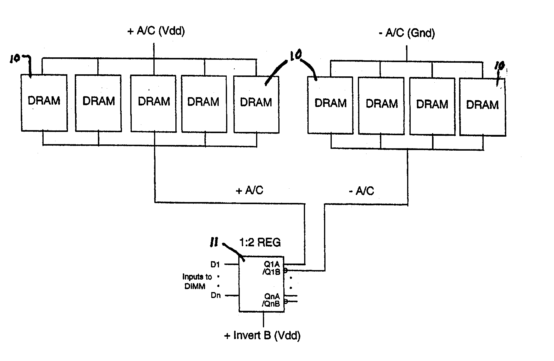
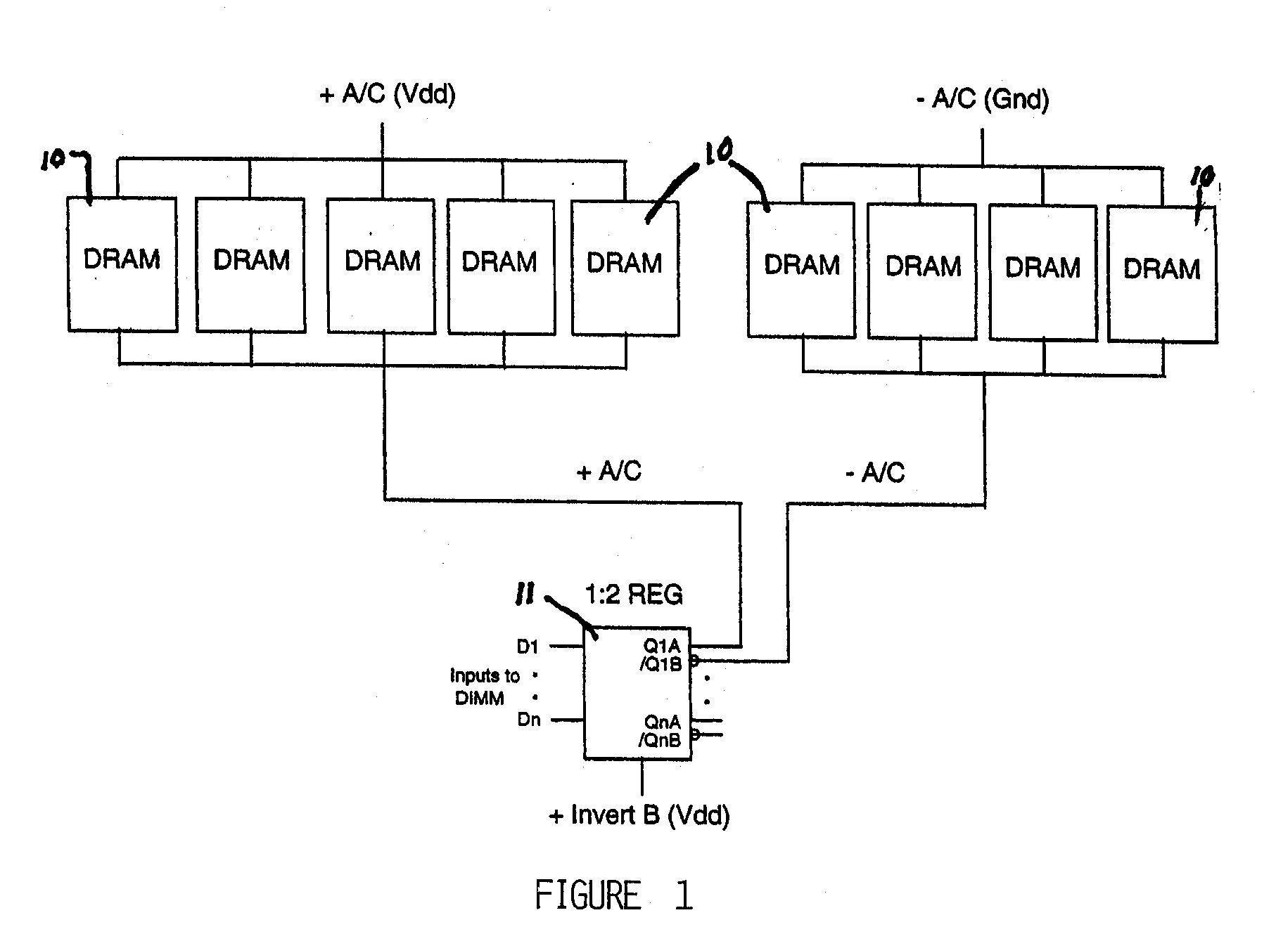
[0022] Attention is directed to FIG. 1 which illustrates the use of the present invention in a DIMM module using a register and DRAM with inverted addre...


PUM


Abstract

A memory system having a plurality of DRAMs which are selectively provided non-inverted or inverted signals. The DRAMs have the ability to accept non-inverted or inverted address/command signals from a register that drives a plurality of signals simultaneously. The system includes DRAM receivers with programmable input polarity and a register with programmable output polarity.

Description

BACKGROUND OF INVENTION [0001] 1. Technical Field [0002] The present invention relates generally to the field of computer memory and more particularly, to multiple synchronous dynamic random access memory (DRAM) systems requiring faster performance. [0003] 2. Background [0004] In recent years, the free fall of processor cycle times to levels well below access times of most dynamic random access memories has generated extensive research and development, the result of which has been the development of several generations of synchronous memory devices. Virtually all previously available semiconductor dynamic random access memory (DRAM) and many static random access memory (SRAM) devices used asynchronous clocking systems in that the clocking signals necessary to perform memory access functions are not synchronized to the associated system processor. Although memories were accessed by signals sent by the processor, the exact time interval between the time a request was sent to a memory ...

Claims


Application Information

Patent Timeline
IPC IPC(8): G06F12/00G06F12/16G11C11/401G11C11/4063
CPCG06F13/4243G11C7/109G11C7/1078
Inventor HAZELZET, BRUCE G.KELLOGG, MARK W.RANKIN, DARCIE J.
Owner MARVELL ASIA PTE LTD
Why Eureka
Try Eureka