Photoresist cleaning solutions and methods for pattern formation using the same
a cleaning solution and photoresist technology, applied in the direction of instruments, non-metal conductors, conductors, etc., can solve the problems of undesired pattern formation in the unexposed area, solubility differences between exposed and undesired patterns, and achieve the effect of preventing the diffusion of generated acid and avoiding undesired photoresist patterns
- Summary
- Abstract
- Description
- Claims
- Application Information
AI Technical Summary
Benefits of technology
Problems solved by technology
Method used
Image
Examples
example 1
Preparation of Cleaning Solutions (1)
[0051] 0.1 g of polyethylene glycol having an average molecular weight of 4,600, and 1,000 g of H2O were mixed and stirred for 1 minute. The resulting mixture was filtered through 0.2 μm filter to obtain a cleaning solution composition of the present invention.
example 2
Preparation of Cleaning Solutions (2)
[0052] 0.1 g of polyethylene glycol monolaurate having an average molecular weight of 3,900, 30 g of ethanol and 970 g of H2O were mixed and stirred for 1 minute. The resulting mixture was filtered through 0.2 μm filter to obtain a cleaning solution composition of the present invention.
example 3
Formation of photoresist pattern (2)
[0054] An underlying layer was formed on a silicon wafer treated with HMDS, and TarF-7a-39 product of TOK Co., Ltd., a methacrylate-type photosensitizer, was spin-coated on the surface of the underlying layer to form a photoresist film at thickness of 3,500 Å. Then, the photoresist film was soft-baked in an oven at 130° C. for 90 seconds. After soft-baking, the photoresist film was exposed to light using an ArF laser exposure device, and 100 mL of the cleaning solution composition obtained from Example 1 was sprayed on the photoresist film from upper portion of a spin device while the silicon wafer was spun on a spin device.
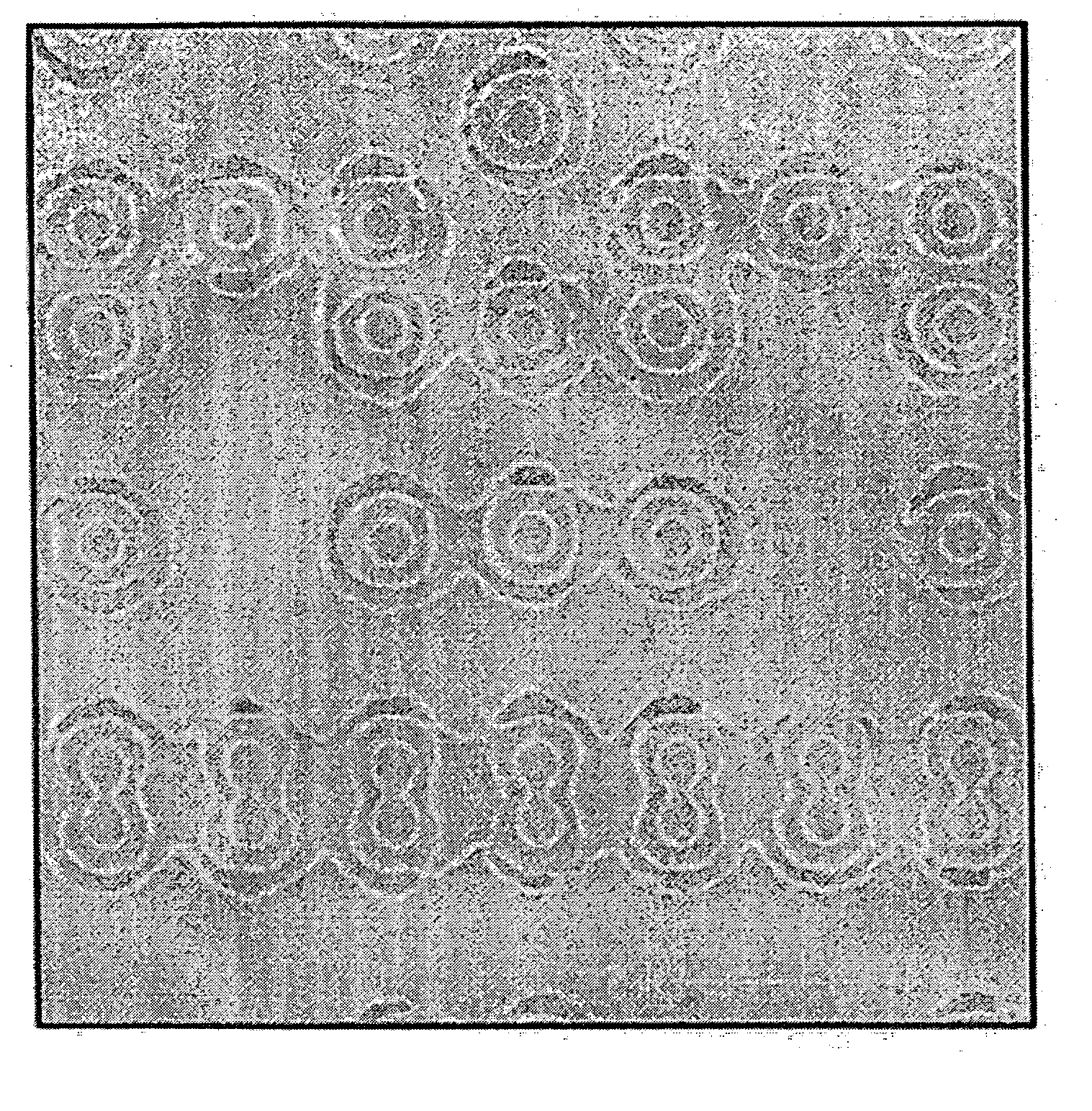
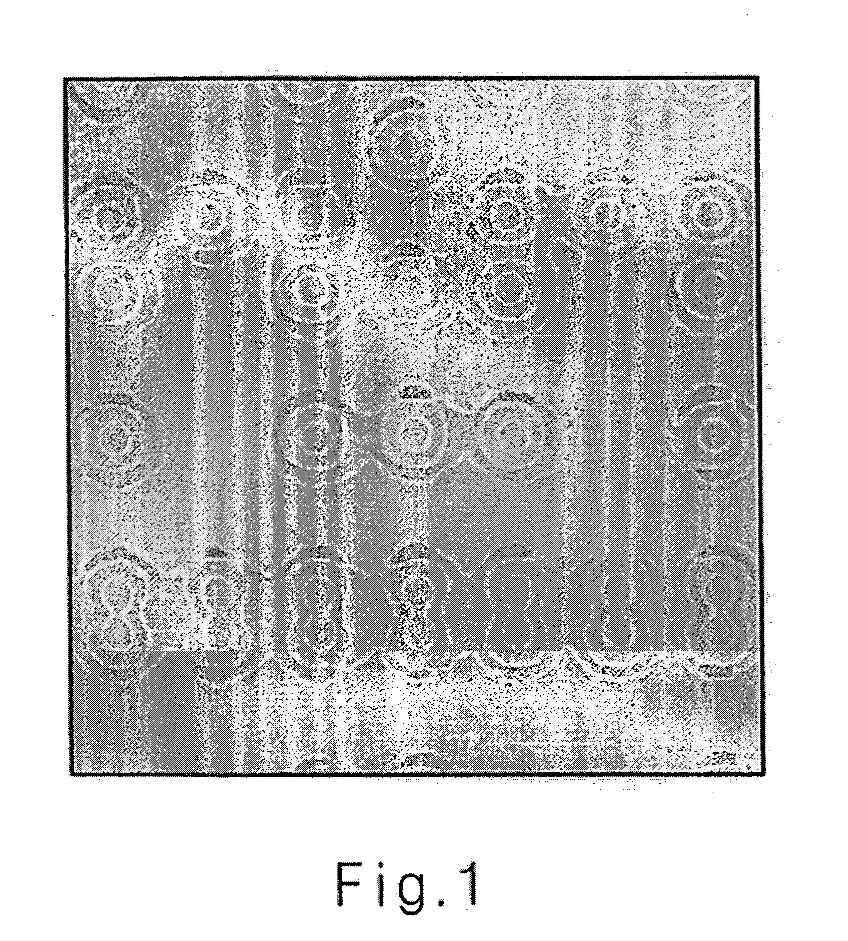
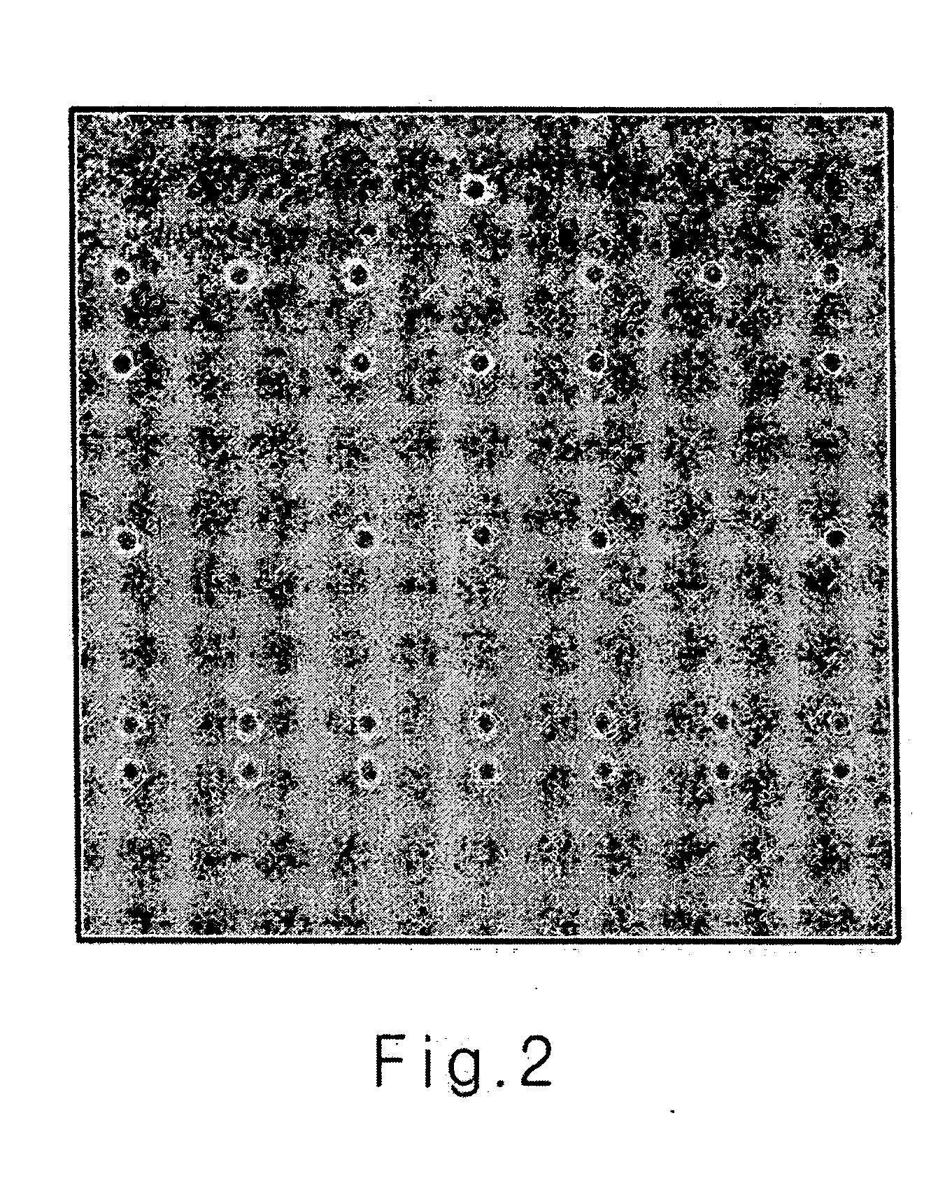
[0055] Then, the photoresist film was post-baked in the oven at 130° C. for 90 seconds, and then developed in a 2.38 wt. % aqueous TMAH solution for 30 seconds to obtain a 150 nm contact hole pattern (see FIG. 2). As a result, it was found that no pattern was formed in the undesired regions in comparison with FIG. 1.
PUM
| Property | Measurement | Unit |
|---|---|---|
| temperature | aaaaa | aaaaa |
| total weight | aaaaa | aaaaa |
| polarity | aaaaa | aaaaa |
Abstract
Description
Claims
Application Information


